NANO BLOG
December 21, 2015 – Sub-60mV-Swing Negative-Capacitance FinFET without Hysteresis Was Demonstrated for the First Time
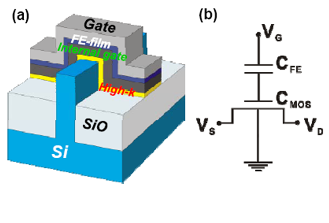
Negative Capacitance FET (NCFET) can be viewed as a FET with built-in voltage amplification. The first ALD ferroelectric HfZrO2 based negative-capacitance FinFET with gate length as small as 30 nm was reported in IEEE International Electron Devices Meeting (IEDM 2015) in Washington, DC USA. Small-signal voltage was amplified by 1.6X maximum at the internal gate with the sub-threshold swing improved from 87 to 55mV/decade. ION increased by >25% for the IOFF.
To read more: IEDM15-621 Paper #22.6.2
“Sub-60mV-Swing Negative-Capacitance FinFET without Hysteresis”
Kai-Shin Li(1), Pin-Guang Chen(2, 3), Tung-Yan Lai1, Chang-Hsien Lin(1), Cheng-Chih Cheng(3), Chun-Chi Chen(1), Yun-Jie Wei(1), Yun-Fang Hou(1), Ming-Han Liao(2), Min-Hung Lee(3), Min-Cheng Chen(1), Jia-Min Sheih(1), Wen-Kuan Yeh(1), Fu-Liang Yang(4), Sayeef Salahuddin(5), Chenming Hu(5)
(1) National Nano Device Laboratories, National Applied Research Laboratories, Hsinchu, Taiwan. (2) Department of Mechanical Engineering, National Taiwan University, Taipei, Taiwan. (3) Institute of Elecro-Optical Science and Technology, National Taiwan Normal University, Taipei, Taiwan. (4) Research Center for Applied Sci., Academia Sinica, Taipei,Taiwan. (5) Dept. of Electrical Eng. and Computer Science, University of California, Berkeley, USA; Tel: +886-3-572-6100 ext. 7706, Fax: +886-3-572-6109, Email: ksli@narlabs.org.tw
(Posted by Yonhua Tzeng)
December 14, 2015 – NIST Measured Nanoscale (16 nm) Features with Fractions of Light (450 nm)
By combining standard through-the-lens viewing with a technique called scatterfield imaging, the NIST team accurately measured patterned features on a silicon wafer that were 30 times smaller than the wavelength of light (450 nanometers) used to examine them. They reported that measurements of the etched lines—as thin as 16 nanometers wide—on the SEMATECH-fabricated wafer were accurate to one nanometer.
credit: NIST/Barnes
(Recommended by Ed Perkins, posted by Yonhua Tzeng)
To read more:
- http://www.nist.gov/pml/div683/measuring_nanoscale_features_fractions_light_12-2-2015.cfm
- J. Qin, R.M. Silver, B.M. Barnes, H. Zhou, R.G. Dixson, and M.A.Henn,”Deep-subwavelength Nanometric Image Reconstruction using Fourier Domain Optical Normalization.” Light: Science & Applications. Article preview Nov. 5, 2015; e16038. To download: http://221.8.12.233/cms/accessory/files/AAP-lsa201638.pdf
June 20, 2015 – Nano Modeling and Simulation – IEEE NTC Technical Committee
The Modeling and Simulation technical committee focuses on topics associated with the formulation, development and use of theoretical models for the understanding and design of nanotechnological systems for engineering applications in a wide spectrum of human society. For this purpose, it addresses technical issues related to the development of numerical codes requiring basic software as well as large-scale computational resources such as density functional theory, tight binding methods, self-consistent Poisson-Schrödinger solver, Monte Carlo simulation, non-equilibrium green function techniques, molecular dynamics to name a few. Among the current and latest topics of investigation are modeling of nanoscale electronic and photonic devices and systems, advanced devices made of new low-dimensionality materials such as graphene and transition metal dichalcogenides, spintronic devices and bio-nanoelectronic devices for molecular manipulation and sensing.
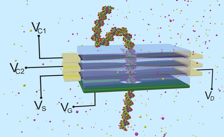
Schematic of a Graphene field effect membrane Transistor containing a nanopore for DNA sequencing (after
Anuj Girdhar, Chaitanya Sathe, Klaus Schulten and Jean-Pierre Leburton, PNAS, 110 (42) pp.1648-1653 (2013))
(Submitted by Jean-Pierre Leburton, posted by Yonhua Tzeng)
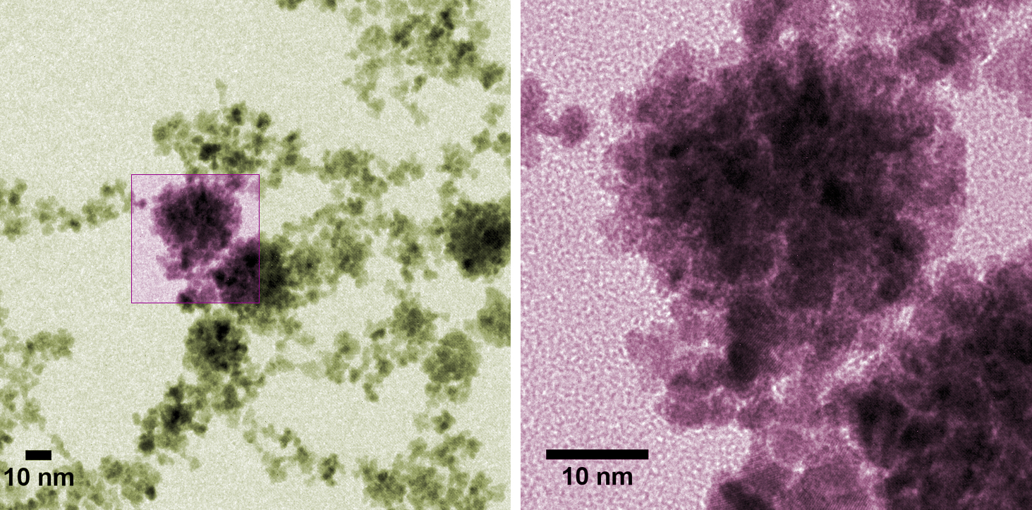
June 10, 2015 – NIST’s ‘Nano-Raspberries’ Could Bear Fruit in Fuel Cells
Researchers at the National Institute of Standards and Technology (NIST) have developed a fast, simple process for making platinum “nano-raspberries”—microscopic clusters of nanoscale particles of the precious metal. The berry-like shape is significant because it has a high surface area, which is helpful in the design of catalysts. Even better news for industrial chemists: the researchers figured out when and why the berry clusters clump into larger bunches of “nano-grapes.”
May 9, 2015 – NIST-led Research Group Creates First Whispering Gallery for Graphene Electrons
Yue Zhao et al., an international team of scientists at the U.S. Commerce Department’s National Institute of Standards and Technology (NIST), demonstrated nanoscale whispering gallery electron resonance in graphene by using the probe voltage of a scanning tunneling microscope to create a circular pn junction in nanoscale area like a circular wall of mirrors to the electrons and similar to what happens to acoustic wave in the famous whispering gallery of St. Paul’s Cathedral.
“An electron that hits the step head-on can tunnel straight through it,” said NIST researcher Nikolai Zhitenev. “But if electrons hit it at an angle, their waves can be reflected and travel along the sides of the curved walls of the barrier until they began to interfere with one another, creating a nanoscale electronic whispering gallery mode.”
The potential of graphene-based quantum electronic resonators and lenses is believed to be huge.
Read the original press release and article: Center for Nanoscale Science and Technology/ NIST ; *Y. Zhao, J. Wyrick, F. Natterer, J. Rodriguez-Nieva, C. Lewandowski, K. Watanabe, T. Taniguchi, L. Levitov, N. Zhitenev, and J. Stroscio. Creating and probing electron whispering-gallery modes in graphene. Science. 8 May 2015: Vol. 348, no. 6235, pp. 672-675. DOI: 10.1126/science.aaa7469.

credit: Jon Wyrick, CNST/NIST
(Recommended by Ed Perkins, posted by Yonhua Tzeng)