NANO BLOG
April 23, 2015 – Probing Johnson noise and ballistic transport in normal metals with a single-spin qubit
Kolkowitz et al. of Harvard University used nitrogen-vacancy centers in diamond to make single-spin qubits for measuring Johnson noise thermally induced in a conductive silver film in the vicinity indicating that nanoscale quantum systems may be controlled by nearby electrodes. Read the original article: Thermally induced electrical currents, known as Johnson noise, cause fluctuating electric and magnetic fields in proximity to a conductor. These fluctuations are intrinsically related to the conductivity of the metal. We use single-spin qubits associated with nitrogen-vacancy centers in diamond to probe Johnson noise in the vicinity of conductive silver films. Measurements of polycrystalline silver films over a range of distances (20 to 200 nanometers) and temperatures (10 to 300 kelvin) are consistent with the classically expected behavior of the magnetic fluctuations. However, we find that Johnson noise is markedly suppressed next to single-crystal films, indicative of a substantial deviation from Ohm’s law at length scales below the electron mean free path. Our results are consistent with a generalized model that accounts for the ballistic motion of electrons in the metal, indicating that under the appropriate conditions, nearby electrodes may be used for controlling nanoscale optoelectronic, atomic, and solid-state quantum systems. Science 6 March 2015: Vol. 347 no. 6226 pp. 1129-1132, DOI: 10.1126/science.aaa4298 (Posted by Y. Tzeng)
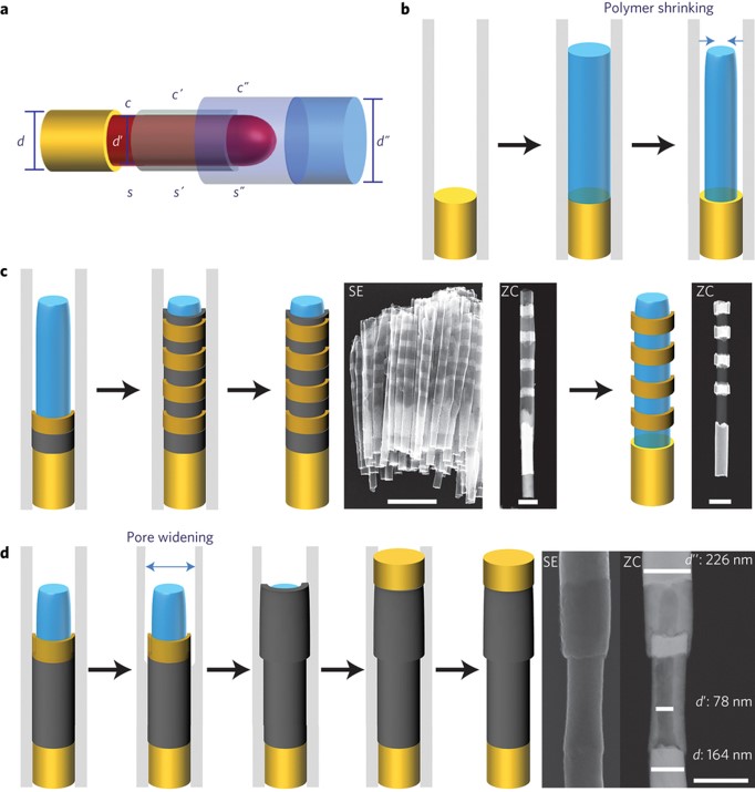
April 23, 2015 – Coaxial Lithography with Sub-10 nm Architectural Control
Tuncay Ozel et al. of Northwestern University demonstrated a core/shell semiconductor nanowire with an embedded plasmonic nanoring, which could not be fabricated by any previously known method, using templated electrochemical synthesis termed as coaxial lithography. Read the original article: Nature Nanotechnology doi:10.1038/nnano.2015.33 (Posted by Y. Tzeng)
April 22, 2015 – Low Energy Loss Cold Electron Transport in Devices Operating at Room Temperature
Professor Koh and his team at University of Texas at Arlington reported in Nature Communication a means of enabling electrons to transport at room temperature like electrons do at very low temperatures with little energy loss by passing electrons through an energy filter made of a quantum well. The team has received funding to apply the discovery to high-density transistors made in the form of nanopillars. Read the original reports: Nanotechnology aids in cooling electrons without external sources, Energy-filtered cold electron transport at room temperature.
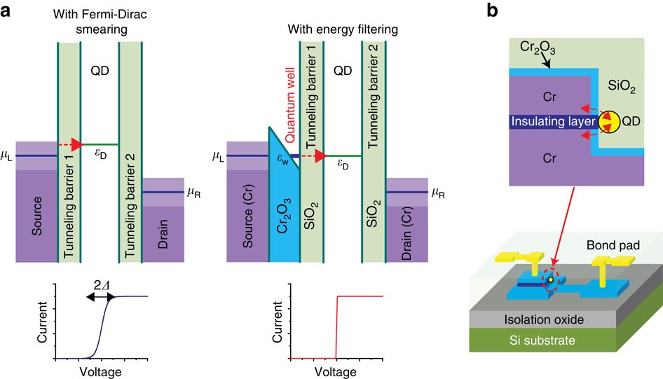
(a) Left: the double-barrier tunnel junction (DBTJ) structure. (a) Right: DBTJ structure with a quantum well inserted between the source and tunnelling barrier 1. (b) Schematic of the DBTJ structure with the energy filter inserted. Top: cross-sectional view. The dotted arrows indicate electron tunnelling paths. Bottom: three-dimensional view of one device unit. The schematics are not to scale. Credit Koh et al., Nature Communication. (Posted by Y. Tzeng)
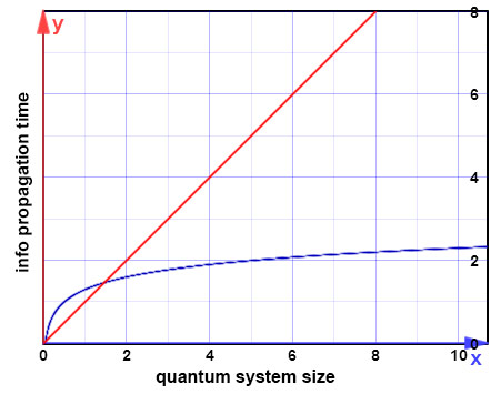
April 14, 2015 – NIST Tightens the Bounds on the Quantum Information ‘Speed Limit’
NIST scientists prove that the propagation time of entanglement between two distant particles for sharing data across a quantum system grows only as a power of the system size instead of logarithmically. The finding implies that quantum processors will be slower than previously predicted. (Posted by Ed. Perkins, Y. Tzeng)
December 16, 2014 – NIST Sensor Enables Self-calibrating AFM
Pressure of light from an optical fiber sets an AFM tip vibrating, of which the movement is measured by an interferometer through another optical fiber giving a value of the probe ‘s stiffness as a means of self-calibration. (Posted by Ed Perkins, Y. Tzeng)
