IEEE Nanotechnology Council
Advancing Nanotech for Humanity
IEEE

NANO BLOG

Meet 2023 IEEE Nano Early Career Award Recipient, Dr Deep Jariwala

Deep Jariwala is an Assistant Professor in Department of Electrical and Systems Engineering at the University of Pennsylvania (Penn). His research interests broadly lie at the intersection of new materials, surface science and solid-state devices for computing, sensing, opto-electronics and energy harvesting applications. Deep completed his undergraduate degree in Metallurgical Engineering from the Indian Institute of Technology, Banaras Hindu University in 2010. Deep went on to pursue his Ph.D. in Materials Science and Engineering at Northwestern University working on charge transport and electronic applications of two-dimensional (2D) semiconductors, graduating in 2015. Deep then moved to Caltech as a Resnick Prize Postdoctoral Fellow from 2015-2017 working on nanophotonic devices and ultrathin solar cells, before joining Penn in 2018 to launch his independent career.

Deep’s research has earned him awards of multiple professional societies including the Russell and Sigurd Varian Award and Paul H. Holloway Award of the American Vacuum Society, The Richard L. Greene Dissertation Award of the American Physical Society, Johannes and Julia Weertman Doctoral Fellowship, the Hilliard Award, the Army Research Office and Office of Naval Research Young Investigator Awards, Nanomaterials Young Investigator Award, TMS Frontiers in Materials Award, Intel Rising Star Award, IEEE Young Electrical Engineer of the Year Award, IEEE Photonics Society Young Investigator Award, IUPAP Early Career Scientist Prize in Semiconductors, IEEE Nanotechnology Council Young Investigator Award in addition to being named in Forbes Magazine list of 30 scientists under 30, is an invitee to Frontiers of Engineering conference of the National Academy of Engineering as well as a recipient of the Sloan Fellowship. Recently, his work on ferroelectric diode memory was also awarded with the Bell Labs Prize. In addition, he has also received the S. Reid Warren Jr. award given to one faculty member every year at Penn Engineering for inspiring and motivating undergraduate students through teaching. He also serves as Associate Editor for IEEE Photonics Technology Letters as well as npj 2D materials and applications. He has published over 100 journal papers with more than 16000 citations and several patents. At Penn he leads a research group comprising more than ten graduate and postdoctoral researchers supported by a variety of government agencies, industries and private foundations.

Google Scholar | Lab website | LinkedIn

Tell us a little bit about your educational/professional background. How are you involved in IEEE NTC Modeling and Simulation?

I grew up in Mumbai, India and went to high school there. I then went to the Indian Institute of Technology at Banaras Hindu University (IIT-BHU) in Varanasi for my bachelor’s degree in Metallurgical Engineering. During my undergraduate degree, I spent two summers at Rice University which sparked my interest in nanotechnology and nanomaterials. After finishing my undergraduate, I went straight to PhD in Materials Science and Engineering at Northwestern University where I worked on novel types of transistors and diodes using two-dimensional (2D) and one-dimensional (1D) semiconductors. During PhD was the first time I got exposed to device modelling and simulation. After PhD, I kept working on devices but moved to Caltech to pursue a postdoctoral position in photonic and optoelectronic devices. At Caltech, I was exposed to the electromagnetic wave and optical simulations. Starting 2018, I moved to the University of Pennsylvania to start my independent research group where we work on both electronic and photonic devices from novel nanomaterials. We make and measure devices as well as simulate and predict their performance.

What is your primary research interest? What are the major areas that your research group works on?

My research interests are extremely broad. But the primary objectives can be summarized as using new materials for novel devices involving computing, communication, sensing and energy harvesting applications. Presently, there are 4 major areas of the research group:

  • Nanoelectronics: In this area, we work on novel logic transistors as well as novel non-volatile memory devices. We also focus on fundamental device challenges such as contact resistance as well as think about circuits and system-level implementation of new devices.
  • Nanophotonics/Optoelectronics: In this area, we focus on low-dimensional materials with novel optical properties and structure them to trap light and observe novel photonic phenomena. We are also equally interested in using the observed novel photonic phenomena in device applications.
  • Functional imaging: In this area, we focus on electron beam and scanning probe-based imaging of new materials, heterostructures and their interfaces. We call this area functional imaging since we are doing more than just standard imaging by applying another stimulus during imaging. For example: applying heat or electric field or magnetic field during e-beam imaging or shining light or applying voltage during scanning probe imaging.
  •  Synthesis of new semiconductor materials: In this area, we use vapour phase and plasma phase deposition techniques to grow new semiconductors and their heterostructures and investigate their fundamental crystal, electronic and optical properties.

Lead us through your Academic Career Highlights and share your experience.

I was always inclined towards high education and deep scientific inquiry. I’d say all the way from my middle school days if my memory serves me correctly. The first major highlight was going to IIT for undergraduate education. There I came in contact with some professors and other senior students who encouraged me to go into research and pointed me in the right direction.

At IIT-BHU, I started doing some molecular dynamics simulations research which led to a summer internship at Rice University. That was another major highlight. The Rice experience opened doors to experimental, physical lab-based research which was very instrumental and eye-opening in terms of my thinking and intellectual evolution. After spending two summers at Rice, I decided to apply for PhD program and was fortunate enough to get into Northwestern University in their Materials Science and Engineering PhD program. That was another major highlight.

Northwestern years were very formative in becoming a well-rounded researcher since my PhD advisers at the time gave me all the freedom and resources and provided a very healthy environment to pursue high-risk, high-reward research. That paid off well which led to a productive PhD and a postdoc opportunity at Caltech. Moving to Caltech to work with one of the leading groups in photonics and optical materials was another major highlight. Caltech experience further developed me into an independent scientist and taught me the importance of collaborations as well as marriage between theory and experiments in research.

All these experiences combined led to my current position as a group leader at Penn. Starting an independent lab and career is always challenging and therefore a major highlight. This experience at Penn taught me a lot about how to raise money, manage ideas, people, resources, collaborations and more importantly expectations of everyone. Doing all this successfully and living through a pandemic was quite an experience. An important positive thing I learned managing our lab through the pandemic is to never give up and always keep motivation high among the students and postdocs. I also learned how resilient most of us are as human beings and emerge from all kinds of adversity. Our group emerged quite strong both mentally and scientifically through the pandemic. We had an excellent 2021 and 2022 in terms of publications which led to several awards and honors for the entire group. A major highlight of all these successes was winning the Bell Labs Prize together with my colleagues Troy Olsson and Eric Stach. That one was a very intense competition and the final round involved presenting in front of a judging panel that had multiple CEOs and Nobel laureates. So that whole experience was quite thrilling.

How is your Research Group structured? Is your work done in collaboration with other Industry Partners? If so, what would be your advice to young researchers on strategies to find a good set of collaborations?

Our research group has a very flat structure. Everyone can approach me directly for any advice or help. Of course, some younger students are mentored by senior students or postdocs but everyone gets to talk to me directly. We work as a team and there are really no boundaries between projects. So, if the nanoelectronics folks think there is something cool on the materials or nanophotonics side that they can contribute to, they just go ahead, talk to the relevant group members and collaborate. Sometimes they would run the ideas by me. Other times it is just spontaneous. Similarly, if they want to collaborate with another group at Penn or elsewhere, I proactively make the connections to get the collaboration going. Similar collaborations work with industry and very important government labs as well. In general, we are a very collaborative group and work with dozens of other researchers all over the world. I personally think that is one of our strengths and what makes us so interdisciplinary and productive.

From the viewpoint of someone who has been in academia for many years, how do you think your perspective or approach to research has changed from when you started your PhD work?

To be honest, I haven’t been in academia for very long. Just finishing ~5 years as a group leader/principal investigator. But my research perspective has changed a lot even in this short time. What I have realized over time is that one should always have a big picture of the impact of the research in their minds while working hard and deeply on a problem. The impact may be in community-wide scientific understanding or in terms of tangible technology. Both are fine and equally important. It is also very important to know when to stop working and let things go/end and when to stop, summarize and publish. Scientific world is very big, getting bigger by the day, and more dynamic and fast-moving these days than ever before. So, one needs to be flexible and adapt to these changes which could be both in ways of doing things or in changes to research problems as well.

Do you or your immediate group focus on translating your research into profitable products or is your group mainly involved in exploring more fundamental questions in nanotechnology? If you address fundamental questions, how does your work differ from work done in the industry?

We do both. I would say in the early parts of my career as a student and postdoc I was mostly a fundamental research person. But nowadays we are quite cognizant that many of our ideas could have commercial value and therefore we frequently patent and also think about licensing or starting companies. In terms of fundamental questions, we are looking at basic materials physics/new phenomena questions which are often not being pursued by most industries. Industries, at least semiconductors and optoelectronic industries are focused on optimizing device performance and scaling. They will pick up a problem in most cases when the physics has already been worked out and individual device or materials performance has exceeded certain set benchmarks that are relevant for a technology/product. We do that kind of research as well but then we try and maintain clear boundaries i.e. if there are things that industries are doing can do much better than us since they have more human power and resources, then we would just stay away from such research problems since they go outside the realm of academia at that point, in my personal opinion.

In an academic research centre such as yours, how do you select a research problem to work on? How do you evaluate progress over time?

This is a great question. Selecting research problems is never an easy process. There are always curiosity-driven questions that one has but the issue is how to find funding and resources to execute them. I, therefore, have two classes of problems. The ones that I am more confident about working with and also confident getting funding for them and other class which are riskier and more difficult to get funding on; but very interesting nonetheless. The former ones are straightforward to work on. Define the problem, get some preliminary data, apply for grants and secure funding (this process can be time-consuming and painful sometimes) and then recruit students and execute. The second class of problems are trickier to work on. Typically, I try and search for discretionary funding opportunities or motivated students and postdocs with their own fellowships to work on such problems. Evaluating progress depends on what you want to learn from the problem or what do want as the final result. If the scientific principle you are after is understood, it means progress has been made and you were successful. However, if the end goal is to reach a certain performance or technology demonstration then once again it is very subjective on how you define it. For all highly applied problems, my personal evaluation is that you develop it to a level that someone can make a real technology and product out of it.

Discuss your IEEE journey and motivation to volunteer.

I joined IEEE when I was PhD student. Mainly because I had heard of it since my high school days. Society was somewhat of an enigma for me during college/undergraduate since I thought it was mainly for circuit engineers. Then after I entered PhD program I realized how broad IEEE is and how many societies and technical councils it had and how interconnected/valuable they are in terms of resources and networking. Thereafter, I regularly started following IEEE activities. I think my involvement with the IEEE intensified when I decided to take up a professorship in the Electrical Engineering (EE) department. I had all my degrees in Materials Science and then I took up EE as my home department, which was very rewarding, to be honest. Then, I got involved in IEEE Young Professionals committees, local EDS chapters, EDS optoelectronics committee etc. I also slowly got involved in NTC and in journal editing for the Photonics Society both of which are very rewarding experiences. I would say that there are multiple places in IEEE where I have found a professional home in. EDS, NTC and the Photonics Society are the three most prominent ones. I would say from the disciplinary perspective my research aligns most closely with NTC. Professional societies are meant for professional development and one way to do that is to contribute to them which is to volunteer. Therefore, I encourage everyone to do so in whatever capacity one can manage.

How do you leverage IEEE for your own learning?

My main sources from IEEE for my own learning and professional development are

  1. Conferences: The content of talks, posters and networking at IEEE conferences is just breathtaking and invaluable.
  2. Journals: I read a lot of papers and also serve as an associate editor which both contribute a lot to learning about other people’s work and hearing the opinions of others in various research areas of interest.
  3. Webinars and committees: IEEE webinars are very well advertised and very informative. Similarly, committee meetings give a great chance to learn not just about society but also about other professionals’ career trajectories in your field as well as outside your field.

Which achievement in IEEE/life are you most proud of?

I have a few achievements related to IEEE that I am very proud of. But the latest honor i.e. being named the IEEE NTC Early Career Awardee for 2023 takes the cake. Given the list of former awardees, how much they have achieved in their own careers and how many of them have had an influence on my own scientific thinking and career, this award from the NTC is truly special.

Figure: Dr. Deep Jariwala receiving the IEEE Nano Early Career 2023 award.

Article Contribution:  This interview was conducted by IEEE NTC MENED 2022 mentee, Miss Noor E Karishma Shaik and reviewed by Prof. M.P.Anantram from IEEE TC-10 Committee.

February 8, 2022 – High-power diamond diodes tested with electronic noise

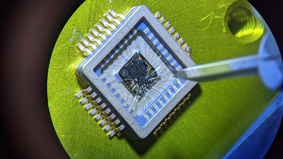
Characterizing defects in diamond devices destined for high-power electronics

Artificially grown diamonds are promising semiconductor materials. Their large energy gap, thermal conductivity, carrier mobility, and other properties make diamonds promising for electronic applications as ultrawide bandgap semiconductors, or UWBGs. However, diamond growth and device fabrication procedures can create defects, inhibiting their function as diodes.

To better assess diamonds for high-power electronics, Ghosh et al. used electronic noise to characterize diamond diode defects. Using grown diamonds, the authors measured low-frequency fluctuations in electrical currents sent through the diamond diodes.

“The measurement of electronic current fluctuations, or electronic noise, can be used to assess the quality of electronic materials and reliability of devices made from such materials,” said co-author Alexander Balandin. “The noise often originates in the non-ideal components or the non-ideal currents of a device. The increase in the noise level can be related to the device failure.”

The results showed the diodes with high and low concentrations of defects had different noise spectra. Additionally, the noise’s dependence on current density could be used to test the quality of the diode.

The authors plan to use the results to create quantitative models that can assess high-power electronics made from diamond and other UWBG semiconductor materials.

“The need for higher power electronics is apparent as we move towards an electrified economy and more energy efficient, interconnected society,” said co-author Robert Nemanich. “The knowledge gained by the ULTRA Center will provide the necessary scientific basis and a co-design ecosystem for a new power electronics economy with ultra-high voltage and current capabilities for highly efficient energy conversion and efficient thermal transport.”

Source: “Excess noise in high-current diamond diodes,” by Subhajit Ghosh, Harshad Surdi, Fariborz Kargar, Franz A. Koeck, Sergey Rumyantsev, Stephen Goodnick, Robert Nemanich, and Alexander A. Balandin, Applied Physics Letters (2022). The article can be accessed at https://doi.org/10.1063/5.0083383.

This paper is part of the Wide- and Ultrawide-Bandgap Electronic Semiconductor Devices Collection, learn more here, published by AIP Publishing.


National Nanotechnology Day (USA)

National Nanotechnology Day (USA)
Event Date: October 09, 2021

National Nanotechnology Day is an annual celebration featuring a series of community-led events and activities on or around October 9 to help raise awareness of nanotechnology, how it is currently used in products that enrich our daily lives, and the challenges and opportunities it holds for the future. This date, 10/9, pays homage to the nanometer scale, 10–9 meters.

Planning for various events and activities is underway at schools, universities, and various organizations around the country. Whether at home or outside, there are so many ways to explore advances in nanotechnology and how it is impacting our everyday lives!

See National Nanotechnology Day | National Nanotechnology Initiative for details.


February 16, 2021 — European Commission GreEnergy Project: nano solar energy harvesting

GreEnergy is a new project funded by the European Commission through the Horizon 2020 Programme aimed at developing optical nano-antennas as cost-effective solar energy harvester for a greener future

Most energy sources we use today have low efficiency, rely on non-renewable resources and cause severe damage to our planet by contributing to global warming. GreEnergy envisions the use of the cleanest energy source available: the sun.  The sun is the world’s most powerful and abundant energy resource, and offers a nearly unlimited supply of energy to our planet. However, according to the Joint Research Centre (JRC), current solar photovoltaics (PV) produce roughly 4% of the world’s electricity, due to their low efficiency and relatively high costs.

GreEnergy’s ambition is to define a new paradigm in the field of solar energy harvesting, by prototyping a self-powering system based on optical nano-antennas which can harvest solar energy, rectify the AC signal and use it to charge a micro-supercapacitor. The targeted overall efficiency of the demonstrators is around 20-40%, which is competitive with respect to the state of the art.

Coordinated by Chalmers University of Technology, GreEnergy is a four-year interdisciplinary project that builds on the expertise of four top-level universities, one research centre and three specialized SMEs coming from 6 different countries, including Chalmers University of Technology (Sweden), Aalto University (Finland), AMO GmbH and IHP – Innovations For High Performance Microelectronics (Germany), NOGAH PHOTONICS Ltd (Israel), SCIPROM Sàrl (Switzerland), Università Politecnica delle Marche and Università di Udine (Italy).

“With GreEnergy we want to demonstrate that it is possible to harvest solar energy more efficiently and at lower cost than what is currently done with photovoltaic cells”, says the project coordinator Prof. Per Lundgren, from Chalmers University of Technology. “It is a real challenge to rectify electromagnetic waves at optical frequencies into a DC current for energy storage and management. This is something we intend to achieve with the coordinated design of the antenna, the rectifier and of the energy storage device for optimal integration. Such an integrated technology has no precedents and will represent a fundamental change in the way that solar energy can be harvested.”

For more info on GreEnergy: visit the GreEnergy website at https://www.greenergy-project.eu


October 09, 2020 – Thermal MagIC: New NIST Project to Build Nano-Thermometers Could Revolutionize Temperature Imaging

Cheaper refrigerators? Stronger hip implants? A better understanding of human disease? All of these could be possible and more, someday, thanks to an ambitious new project underway at the National Institute of Standards and Technology (NIST).

NIST researchers are in the early stages of a massive undertaking to design and build a fleet of tiny ultra-sensitive thermometers. If they succeed, their system will be the first to make real-time measurements of temperature on the microscopic scale in an opaque 3D volume — which could include medical implants, refrigerators, and even the human body.

The project is called Thermal Magnetic Imaging and Control (Thermal MagIC), and the researchers say it could revolutionize temperature measurements in many fields: biology, medicine, chemical synthesis, refrigeration, the automotive industry, plastic production — “pretty much anywhere temperature plays a critical role,” said NIST physicist Cindi Dennis. “And that’s everywhere.”

Measuring and controlling temperature in 3D is highly desirable for medical diagnostics, precision manufacturing, and much more. However, there is currently no way to measure 3D temperature inside these kinds of systems. NIST researchers are working on a solution using tiny nanoscale thermometers. Credit: Sean Kelley/NIST. Music: Blue Dot Sessions.The NIST team has now finished building its customized laboratory spaces for this unique project and has begun the first major phase of the experiment.

Thermal MagIC will work by using nanometer-sized objects whose magnetic signals change with temperature. The objects would be incorporated into the liquids or solids being studied — the melted plastic that might be used as part of an artificial joint replacement, or the liquid coolant being recirculated through a refrigerator. A remote sensing system would then pick up these magnetic signals, meaning the system being studied would be free from wires or other bulky external objects.

The final product could make temperature measurements that are 10 times more precise than state-of-the-art techniques, acquired in one-tenth the time in a volume 10,000 times smaller. This equates to measurements accurate to within 25 millikelvin (thousandths of a kelvin) in as little as a tenth of a second, in a volume just a hundred micrometers (millionths of a meter) on a side. The measurements would be “traceable” to the International System of Units (SI); in other words, its readings could be accurately related to the fundamental definition of the kelvin, the world’s basic unit of temperature.

The system aims to measure temperatures over the range from 200 to 400 kelvin (K), which is about -99 to 260 degrees Fahrenheit (F). This would cover most potential applications — at least the ones the Thermal MagIC team envisions will be possible within the next 5 years. Dennis and her colleagues see potential for a much larger temperature range, stretching from 4 K-600 K, which would encompass everything from supercooled superconductors to molten lead. But that is not a part of current development plans.

“This is a big enough sea change that we expect that if we can develop it — and we have confidence that we can — other people will take it and really run with it and do things that we currently can’t imagine,” Dennis said.

Potential applications are mostly in research and development, but Dennis said the increase in knowledge would likely trickle down to a variety of products, possibly including 3D printers, refrigerators, and medicines.

1 2 7