NANO BLOG
February 24, 2020 – Simple Retrofit Transforms Ordinary Electron Microscopes Into High-Speed Atom-Scale Cameras
National Institute of Standards and Technology (NIST)
February 24, 2020
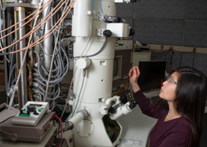 Researchers at the National Institute of Standards and Technology (NIST) and their collaborators have developed a way to retrofit the transmission electron microscope — a long-standing scientific workhorse for making crisp microscopic images — so that it can also create high-quality movies of super-fast processes at the atomic and molecular scale. Compatible with electron microscopes old and new, the retrofit promises to enable fresh insights into everything from microscopic machines to next-generation computer chips and biological tissue by making this moviemaking capability more widely available to laboratories everywhere.
“We want to be able to look at things in materials science that happen really quickly,” said NIST scientist June Lau. She reports the first proof-of-concept operation of this retrofitted design with her colleagues in the journal Review of Scientific Instruments. The team designed the retrofit to be a cost-effective add-on to existing instruments. “It’s expected to be a fraction of the cost of a new electron microscope,” she said.
Read full article at NIST here.
August 31, 2017 – Photon-triggered nanowire transistors are reported in Nature Nanotechnology
Kim et al., recently reported on photon-triggered nanowire (NW) transistors, a new step toward optical computing. These devices consist of crystalline silicon (CSi) NWs that include (PSi) segments in the middle and electrical contacts at both ends of the NW. The PSi acts as a reservoir and supplies carriers to the CSi channel when is exposed to light. It allows for an on/off ratio as high as 8×10⁶. Based on this method authors also demonstrated photon-triggered logic gates and a sub-micron resolution photodetector system.
![]()
To read more: https://www.nature.com/nnano/journal/vaop/ncurrent/full/nnano.2017.153.html
(Contents prepared by Dr. Noelia Vico Trivino and posted by Jr-Hau (JH) He)
August 31, 2017 – Nanophotonic Atomic Force Microscope (AFM) transducers enable chemical composition and thermal conductivity measurements at the nanoscale
A near-field cavity optomechanics readout concept has been integrated with picogram-scale probes to realize fully functional AFM detection. This allows achieving high temporal resolution (<10 ns) and picometer vertical displacement uncertainty simultaneously, breaking the trade-off between AFM measurement precision and ability to capture transient events.
Adapted with permission from Nano Lett., Article ASAP, DOI: 10.1021/acs.nanolett.7b02404. Copyright © 2017 American Chemical Society.
To read more: http://pubs.acs.org/doi/abs/10.1021/acs.nanolett.7b02404
(Contents prepared by Dr. Noelia Vico Trivino and posted by Jr-Hau (JH) He)
February 23, 2016 – Microtubules propelled by surface-adhered kinesin motors perform biocomputationAn international team of researchers has made a breakthrough in the field of biocomputation.
By exploiting microtubules propelled by surface-adhered kinesin motors as motile nanoscale agents capable of performing basic computations, the subset sum problem was solved in a highly parallel approach. For more information, see Nicolau Jr. et al. in the Early Access Section of the Proceedings of the National Academy of Sciences:

To read more: http://www.pnas.org/content/early/2016/02/17/1510825113
(Contents prepared by H. Hess and posted by Y. Tzeng.)
December 25, 2015 – 2-D dichalcogenide MoS2 with PL QY of more than 95% is reported in Science
Amani et al. recently reported near-perfect two-dimensional transition metal dichalcogenide, MoS2 with photoluminescence quantum yield of more than 95% by chemical treatment in a nonoxidizing organic superacid: bis(trifluoromethane) sulfonimide (TFSI), which eliminates defect-mediated nonradiative recombination.
To read more: Near-unity photoluminescence quantum yield in MoS2. Matin Amani, Der-Hsien Lien, Daisuke Kiriya, Jun Xiao, Angelica Azcatl, Jiyoung Noh, Surabhi R. Madhvapathy, Rafik Addou, Santosh KC, Madan Dubey, Kyeongjae Cho, Robert M. Wallace, Si-Chen Lee, Jr-Hau He, Joel W. Ager III, Xiang Zhang, Eli Yablonovitch, Ali Javey. Science 27 November 2015: Vol. 350 no. 6264 pp. 1065-1068, DOI: 10.1126/science.aad2114
(Posted by Yonhua Tzeng)