Distinguished Lecturers 2023
The IEEE NTC is pleased to announce the appointments of Distinguished Lecturers for 2023.
Talks by NTC Distinguished Lecturers can be requested by: IEEE student branches; NTC or member Society Chapters; NTC and member Society Conferences; conferences of other IEEE Societies not members of the NTC for major plenary/keynote (based on availability of funding). Please contact the presenter directly to arrange for a presentation.
| DL Name |
Topic(s) |
| Xiangfeng Duan | 1. 2D Transistors: Promises, Problems, and Prospects |
| Zetian Mi | 1. Nanoscale and Quantum Engineering of III-nitrides for High Efficiency UV Optoelectronics and Micro LEDs |
| Jiming Bao | 1. Cubic Boron Arsenide (cBAs): a Promising Semiconductor for Next Generation Electronics |
| Xiaoying Zhuang | 1. Machine Learning Based Multiscale Exploration and Characterization of 2D materials |
| Li Tao | 1. Emerging Low dimensional Materials and Devices for Wearable IoTs and Healthcare Applications in the Post Moore Era |
| Zenghui Wang | 1. A Vibrant New World Exploring New Physics and Materials with Nanoelectromechanical Systems (NEMS) |
| Antonio Di Bartolomeo* | 1. Electrical transport measurements in 2D materials 2. Nanotransistors 3. 2D Materials: fabrication, properties and applications |
| Weida Hu* | 1. Nanoscale infrared photodetectors manipulated by localized fields |
| Kin Fong Lei* | 1. Analyses of Molecular Expression of Cancer Cells Cultured in Stacking Nanofiber Substrate 2. Impedimetric Monitoring of Cancer Cell Responses in Three-dimension Culture Environment |
| Aida Todri-Sanial* | 1. Novel devices and circuits design methods energy efficient neuromorphic computing with oscillatory neural networks |
| Massimiliano Di Ventra* | 1. Quantum transport in nanoscale systems 2. MemComputing: Fundamentals and Applications 3. Next-generation sequencing with nanochannels 4. Industrial research from an academic point of view |
| Yang Xu* | 1. Graphene/Silicon Heterojunctions for Integrated Nanotechnology |
| Ken-Tye Yong* | 1. Nanocarbons for Biology and Medicine: Sensing, Imaging, and Drug Delivery |
| Yong Zhu* | 1. Nanomaterial-Enabled Soft Electronics 2. MEMS for Characterizing Mechanical and Coupled Properties of Nanomaterials |
| * Re-appointment for second year. | |
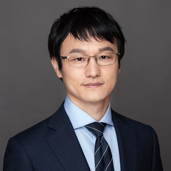
 Xiangfeng Duan
UCLA, Department of Chemistry and Biochemistry, CA, USA
E-Mail: xduan@chem.ucla.edu
Distinguished Lecturer Talk Title:
2D Transistors: Promises, Problems, and Prospects
Abstract:
Two-dimensional (2D) semiconductors have attracted tremendous interest as atomically thin channels for continued transistor scaling. However, despite many proof-of-concept demonstrations, the full potential of 2D transistors remains elusive. To this end, the fundamental merits and technological limits of 2D transistors need a critical assessment, reality check, and objective projection. In this talk, I will briefly review the promises and the current status of 2D transistors, and highlight the widely used device parameters (e.g., carrier mobility, contact resistance) could be frequently misestimated or misinterpreted, and may not be the most reliable performance metrics for benchmarking 2D transistors. We suggest the saturation or on-state current density, especially in the short channel limit, could provide a more reliable measure for assessing the potential of diverse 2D semiconductors, and should be applied for cross-checking different studies, especially when milestone performance metrics are claimed. I next summarize the critical technical challenges and current status in optimizing the channel, contacts, dielectric, and substrate interfaces and outline the potential pathways to push the limit of 2D transistors; lastly conclude with a prospect on the critical technical targets, the key technological hurdles to enable the lab-to-fab transition, and the potential opportunities arising in these atomically thin semiconductors.
Highly stretchable van der Waals thin-films for adaptable and breathable electronics
The integration of electronic systems with irregular, soft objects is of increasing interest for many emerging electronic applications including ubiquitous electronics for internet of things and bioelectronics intimately interacting with living organisms. Although the hard inorganic materials can be made flexible in the ultrathin membrane format, they are hardly stretchable and fundamentally incapable of forming conformal interface with irregular geometries with non-zero Gaussian curvatures due to the topological limitations. Here I introduce a unique design of highly stretchable van der Waals thin films (VDWTFs) for microscopically adaptable membrane electronics. Assembled from solution-processable two-dimensional (2D) nanosheets, the VDWTFs feature bond-free vdW interactions among the staggered nanosheets, with a sliding and rotation degree of freedom between neighbouring nanosheets to ensure extraordinary mechanical flexibility, stretchability, malleability and adaptability to irregular surface topographies. Additionally, the staggered nanosheet architecture features a highly interconnected percolation network of nanometre-scale channels with an excellent permeability. The freestanding VDWTFs show an excellent mechanical match with soft biological tissues, naturally adapting to microscopic topographies and directly merging with dynamically changing organisms with highly conformal interfaces, endowing living organisms with electronic functions, including leaf-gate and skin-gate VDWTF transistors. With excellent conformability and adaptability to skin textures, the skin transistors allow for high fidelity monitoring skin potentials and electrophysiological signals with excellent signal-to-noise ratio and superior immunity to motion artifacts. The VDWTFs thus define a new platform of electronic membranes readily adaptable to different form factors, and can open up exciting opportunities for many emerging electronic applications.
High-Order Van Der Waals Superlattices and Artificial Quantum Solid Beyond Mechanical Exfoliation and Restacking
The advent of two-dimensional atomic crystals (2DACs) and van der Waals heterostructures (vdWHs) has inspired a new thinking on heterostructure construction beyond the limits of lattice matching requirement. However, the vdWHs explored to date have been largely limited to relatively simple systems with a small number of building blocks. The preparation of high-order vdW superlattices with a larger number of alternating units is exponentially more challenging due to the limited yield and scalability of the commonly used exfoliation-and-restacking strategy. Here I will discuss strategies to create high-order vdW superlattices (vdWSLs). First, by exploiting a capillary-force-driven rolling-up process, we show a series of synthetic VDWHs can be transformed into high-order vdWSLs with alternating atomic layers of widely variable material compositions, electronic band offset dimensions, chirality and topology. Alternatively, we further introduce a molecular intercalation approach to prepare a new family of hybrid superlattices consisting of alternating layers of covalently bonded 2D atomic layers and self-assembled molecular layers, which opens the door to exploit highly versatile molecular design strategies to tailor solid-state materials, enabling artificial materials with designable structural motifs and tunable electronic properties beyond the reach of conventional crystalline solids. We will particularly highlight a recent example of a new class of chiral molecular intercalation superlattices with robust chiral-induced spin selectivity. The formation of high-order vdW superlattices defines a rich artificial materials platform to unlock previously inaccessible physical limits and enable new device concepts beyond the reach of the existing materials.
Bio:
Dr. Duan received his B.S. Degree from University of Science and Technology of China in 1997, and Ph.D. degree from Harvard University in 2002. He was a Founding Scientist and then Manager of Advanced Technology at Nanosys Inc., a nanotechnology startup founded based partly on his doctoral research. Dr. Duan joined UCLA with a Howard Reiss Career Development Chair in 2008, and was promoted to Associate Professor in 2012 and Full Professor in 2013. Dr. Duan’s research interest includes nanoscale materials, devices and their applications in future electronic and energy technologies. Dr. Duan has published over 300 papers with over 85,000 citations, and holds >50 issued US patents. Dr. Duan has received many awards for his pioneering research in nanoscale science and technology, including MIT Technology Review Top-100 Innovator Award, NIH Director’s New Innovator Award, NSF Career Award, Alpha Chi Sigma Glen T. Seaborg Award, Herbert Newby McCoy Research Award, US Presidential Early Career Award for Scientists and Engineers (PECASE), ONR Young Investigator Award, DOE Early Career Scientist Award, Human Frontier Science Program Young Investigator Award, Dupont Young Professor, Journal of Materials Chemistry Lectureship, International Union of Materials Research Society and Singapore Materials Research Society Young Researcher Award, the Beilby Medal and Prize, the Nano Korea Award, International Society of Electrochemistry Zhao-Wu Tian Prize for Energy Electrochemistry, Science China Materials Innovation Award, AIP Horizons Lectureship, NanoMaterials Science Young Scientist Award, Materials Research Society Middle Career Researcher Award and most recently IEEE Pioneer Award in Nanotechnology. He is currently an elected Fellow of Royal Society of Chemistry and Fellow of American Association for the Advancement of Science.
URL: http://xduan.chem.ucla.edu
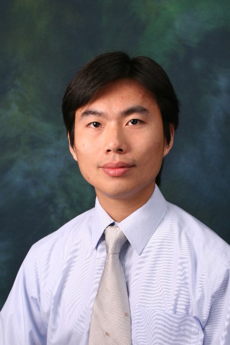
 Zetian Mi
Department of Electrical Engineering and Computer Science, University of Michigan, USA
E-Mail: ztmi@umich.edu
Distinguished Lecturer Talk Title:
Nanoscale and Quantum Engineering of III-nitrides for High Efficiency UV Optoelectronics and Micro LEDs
Abstract:
Microscale light emitting diodes (micro-LEDs), as well as LEDs and laser diodes operating in the mid and deep ultraviolet (UV), have emerged as the frontier of semiconductor optoelectronics and are poised to revolutionize mobile displays, virtual/augmented reality, water purification, sterilization, and many other critical applications. The achievement of high efficiency micro-LEDs and UV optoelectronics, however, has remained extremely challenging, due to materials imperfection of conventional III-nitride quantum wells. Here, I will present recent advances of nanoscale and quantum engineering of III-nitride heterostructures that can fundamentally break the efficiency bottleneck of micro-LEDs and deep UV optoelectronics. Due to the efficient surface strain relaxation, III-nitride nanostructures exhibit significantly reduced dislocation densities compared to their conventional quantum well counterparts. Our studies have further shown that p-type Mg-dopant incorporation is much more efficient in nanostructures. These attributes have been exploited to realize high efficiency micro-LEDs operating in the deep visible (green and red) and to achieve relatively efficient LEDs operating in the UV-C spectra. Moreover, the three-dimensional quantum confinement of charge carriers can drastically reduce the transparency carrier density of ultrawide bandgap semiconductors, leading to, for the first time, electrically pumped mid and deep UV laser diodes with ultralow threshold operation.
Bio:
Zetian Mi is a Professor in the Department of Electrical Engineering and Computer Science at the University of Michigan, Ann Arbor. He received the PhD degree in Applied Physics at the University of Michigan in 2006. His teaching and research interests are in the areas of low dimensional semiconductors and their applications in photonic, electronic, clean energy, and quantum devices and systems. He was a faculty member at McGill University from 2007 to 2016, where he received several awards, including the Hydro-Québec Nano-Engineering Scholar Award in 2009, the William Dawson Scholar Award in 2011, the Christophe Pierre Award for Research Excellence in 2012, and the Engineering Innovation Award in 2015. Prof. Mi has received the Science and Engineering Award from W. M. Keck Foundation in 2020 and the David E. Liddle Research Excellence Award in 2021. Prof. Mi has also received the Young Investigator Award from the 27th North American Molecular Beam Epitaxy (MBE) Conference in 2010, the Young Scientist Award from the International Symposium on Compound Semiconductors in 2015, and the IEEE Photonics Society Distinguished Lecturer Award in 2020. Prof. Mi currently serves as the Editor-in-Chief of Progress in Quantum Electronics, Serial Editor of Semiconductors and Semimetals, and Vice President for Conferences of IEEE Photonics Society. Prof. Mi has served as the Chair of many international conferences, including the General Chair of IEEE Photonics Society Summer Topicals Meeting in 2016-2017, Program Chair of 30th North American Conference in 2013, Co-Chair of International Symposium on Semiconductor Light Emitting Devices in 2017, General Chair of IEEE Photonics Conference in 2020, and Program Chair of Compound Semiconductor Week in 2022. Prof. Mi is a fellow of IEEE, APS, Optica, and SPIE. Prof. Mi is a co-founder of NS Nanotech, Inc. and NX Fuels, Inc.
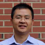
 Jiming Bao
Cullen College of Engineering Building, University of Houston, TX, USA
Email: jbao@uh.edu
Distinguished Lecturer Talk Title:
Cubic Boron Arsenide (cBAs): a Promising Semiconductor for Next Generation Electronics
Abstract:
Cubic boron arsenide (c-BAs) is an indirect bandgap (1.82 eV) semiconductor, it has a similar band structure as silicon, but its thermal conductivity is 10 times higher and its carrier mobility is three times larger at room temperature. This suitable bandgap, simultaneous high thermal conductivity and high carrier mobility have made c-BAs a promising material for next generation electronics, especially after recent experimental verifications of these excellent thermal and electronic properties. However, many challenges still remain in order for c-BAs to realize its many promises. Besides the challenge of synthesis of uniform large size c-BAs crystals, techniques that can rapidly characterize and screen high quality c-BAs are still lacking. In this talk, I will first give a brief introduction to the history and basic properties of c-BAs, I will then explain its next-only-to-diamond high thermal conductivity. After that, I will show optical techniques that have been developed to measure thermal conductivity and carrier mobility. Finally I will show photoluminescence and Raman spectra of c-BAs, and discuss the challenges of using them to identify and characterize high quality c-BAs.
Bio:
Jiming Bao is a professor of Electrical and Computer Engineering at the University of Houston. He graduated from Zhejiang University with B.S. and M.S. in Physics. He obtained his Ph.D. in Applied Physics in 2003 from the University of Michigan under Roberto Merlin; he then did post-doctoral research in Federico Capasso’s group at Harvard University before joining the University of Houston in 2008 as an assistant professor. Dr. Bao is interested in developing and understanding new nanomaterials and then exploring their novel applications in energy, optoelectronics and sensing. Dr. Bao is a Fellow of the Optical Society of America (OSA) and American Physical Society (APS).
 Xiaoying Zhuang
Faculty of Mathematics and Physics, Institute of Photonics, Leibniz University Hannover, Germany
Email: zhuang@iop.uni-hannover.de
Distinguished Lecturer Talk Title:
Machine Learning Based Multiscale Exploration and Characterization of 2D materials
Abstract:
2D materials have attracted widespread attention in recent years. They have some unique properties that other usual materials do not have. For example, its electrical, mechanical, thermal and optical properties vary with the number of layers. Density functional theory (DFT) calculations are robust tools to explore the physical properties of pristine structures as well as to explore new type of 2D nanomaterials at their ground state, but they become exceedingly expensive for large systems or at finite temperatures. Classical molecular dynamics (CMD) simulations offer the possibility to study larger systems at elevated temperatures, but they require accurate interatomic potentials. We developed machine-learning interatomic potentials (MLIPs) passively fitted to computationally inexpensive ab-initio datasets which can be used to evaluate the complex physical properties of nanostructured materials, with only a fractional computational cost of conventional DFT-based solutions, cutting down from months to tens of hours. MLIPs offer extraordinary capabilities to marry the first-principles accuracy with multiscale modeling and thus enable the modeling of complex nanostructures at continuum level and has flexibility without paying unaffordable computational costs. We show outstanding and robust potential to develop fully automated platforms, to design, optimize and explore various properties of 2D materials and structures at continuum level, and with inherent precision and robustness.
Bio:
Dr. Xiaoying Zhuang’s is among the leading and renowned scientists in the field of modeling and simulation (or Simulation Based Engineering Science) and its application to challenging problems in engineering and materials science, especially the computer-aided design of new nanocomposites and nanostructure. Her highly interdisciplinary research combines the areas of scientific computing, nanotechnology, mechanics, applied mathematics and materials science. Her contributions did not have only a major impact within the academic community, but they were also used commercially to tackle difficult and highly complex problems, such as the computer-assisted development of new materials. Dr. Xiaoying Zhuang’s work in the field of computer-assisted nanostructure and nanomaterials design, which she is meanwhile pursuing for around a decade, is truly seminal and groundbreaking. Dr. Xiaoying Zhuang’s recently developed groundbreaking work on ‘Machine learning (ML) based potentials’ and adaptive multi-scale modeling has laid the foundation for performing calculations from the smallest quantum mechanical scale (due to the highly precise and extremely efficient ML potentials) up to the macro-scale. For graphene/borophene heterostructures she has already convincingly proven the accuracy of these predictions. Because of these pioneering developments, a drastic improvement in the development of new, more complex materials can be expected in the foreseeable future.
Dr. Zhuang’s very extensive and pioneering research in this area is an important step towards a new paradigm for the efficient use of computational methods for the development of new materials. Her revolutionary paradigm, which she developed and implemented for novel carbon-reinforced polymer-matrix composites as well as flexoelectric energy harvesters, has been awarded with two prestigious awards: the Sofia Kovaleskaja Award (2015 on polymer-matrix composites) and the ERC Starting Grant (2019 on flexoelectric energy converters). Prof. Zhuang had already proven that such approaches are suitable for the development of new materials. Her models and simulations have already led to the development of a new ‘nano-coating’ called LUMA (in 2016), which has already been fabricated and applied commercially.
 Li Tao
School of Materials Science and Engineering, Southeast University, China
Email: tao@seu.edu.cn
Distinguished Lecturer Talk Title:
Emerging Low dimensional Materials and Devices for Wearable IoTs and Healthcare Applications in the Post Moore Era
Abstract:
Low-dimensional atomic sheets yield collective properties of mechanical flexibility and tunable bandgap for innovative flexible micro-nano devices and systems. This talk will introduce silicene transistors, bismuthene devices and boron nitride (BN) quantum dots as representatives of low-dimensional materials for flexible/wearable electronics. Our effort in a unique nanofabrication approach allows silicene transistor make its debut, corroborating theoretically predicted ambipolar transport with Dirac band structure. This requires a careful engineering of the number of layers of silicene and its interface in between source/drain electrodes and capping dielectrics, stabilizing and preserving silicene during transfer and device fabrication. This talk also highlights our recent experimental progress on the synthesis, characterization and device integration on bismuthene and hBN. We demonstrated a Vis-NIR photodetector with μs response enabled by bismuthene/Si(111) heterolayer. In a similar strategy of surface state tuning via amination degree, hBN quantum dots have been implemented with full-color emission (420−610 nm) and quantum yield over 32.27%. Owing to its unique thermal stability, hBN quantum dots hold great potential for flexible display, optoelectronic and various other applications.
Bio
Professor Li Tao obtained bachelor’s degree from Southeast University in 2004, and received his Ph.D. degree from the University of Texas at Dallas in 2010. Then, he entered the University of Texas at Austin Microelectronics Research Center for post-doctoral research and was promoted to research scientist in 2012. He joined Southeast University as a professor of Materials Science and Engineering in 2016. Prof. Tao’s research interests include nanofabrication, two-dimensional semiconductor materials and devices, and the cross-application of micro-systems and nanotechnology in healthcare and IoTs. He has over 50 publications, including first/corresponding author Nature Nanotechnology (citations>1000), Chemical Society Reviews, IEEE TAP, Infomat etc. He serves as associate editors for Research (the first Science Partner Journal) and MicroElectronics Engineering. Prof. Tao has delivered more than 15 invited talks in IEEE, MRS, APS and other conferences, and served as the conference general chair for IEEE NMDC 2020&2022. He is a senior member of IEEE.
 Zenghui Wang
Institute of Fundamental and Frontier Sciences, University of Electronic Science and Technology, China
Email: zenghui.wang@uestc.edu.cn
Distinguished Lecturer Talk Title:
A Vibrant New World Exploring New Physics and Materials with Nanoelectromechanical Systems (NEMS)
Abstract:
The advent of low-dimensional nanostructures has enabled a plethora of new devices and systems. Among them, nanoelectromechanical systems (NEMS) offer the unique capability of coupling exquisite material properties found in these atomically-defined nanostructures with their mechanical degree of freedom, opening new opportunities for exploring exotic phenomena at the nanoscale. In particular, as these devices are driven into mechanical vibration—just like musical instruments—they become essentially nanoscale guitars, drums, tuning folks, and so on. By studying the infinitesimal mechanical vibrations in these minuscule “music instruments”, i.e., listening to the “sound of music” at the nanoscale, researchers can study a number of fundamental physical processes such as absorption, phase transition, anisotropy, and nonlinear processes, and can explore the opportunity of building novel nanodevices for applications such as sensing, computing, and signal processing.
Bio:
Max Zenghui Wang is currently a professor at the University of Electronic Science and Technology of China (UESTC). His research interests and expertise primarily focus on nanoscale devices and systems, particularly Nanoscale Resonators, and High-Frequency Resonant Sensors & Transducers. He earned a Ph.D. degree (2010) from University of Washington, Seattle, and conducted research at Cornell University and Case Western Reserve University before joing UESTC. He has published dozens of research articles in journal such as Science, Nature Physics, Nature Nanotechnology, Nature Communications, and Science Advances. He has given dozens of invited talks and seminars at peer-reviewed conferences and research universities. He is an IEEE senior member, and has been serving on the Technical Program Committees for IEEE MEMS, IEEE IFCS, IEEE NANO, IEEE NEMS, IEEE NMDC, Transducers, and the MEMS/NEMS Technical Group at the American Vacuum Society (AVS) International Symposium and Exhibition.
 Antonio Di Bartolomeo
Physics Department “E. R. Caianiello”, University of Salerno, Italy
E-Mail: adibartolomeo@unisa.it
Distinguished Lecturer Talk Title(s):
1. Electrical transport measurements in 2D materials
2. Nanotransistors
3. 2D Materials: fabrication, properties and applications
Abstract:
Two-dimensional materials hold great promise for future nanoelectronics. Their atomic thickness enables highly scaled field-effect transistors with reduced short-channel effects and relatively high carrier mobility that are essential for high-performance, low-voltage device operations. The electrical transport properties of 2D materials are mainly investigated using back-gated field-effect devices, for which conventional electrical characterization methods can produce unreliable results. The formation of low-resistance contacts and the control of process-induced defects or interface states are among the main challenges to solve for the study of intrinsic electrical transport of 2D materials. The accurate characterization of parameters such as conductivity, carrier density, mobility, contact resistance, Schottky barriers, interface trap density, etc. is very important for the progress in the field. In this lecture, I’ll highlight the main issues related to the electrical characterization of 2D materials and I’ll review the electrical measurements techniques that are commonly applied to 2D-based field-effect transistors, such as current–voltage (I–V) characterization, 2- and 4-point probe measurements, Hall-effect measurements, transmission line method and capacitance–voltage (C-V) measurements. I will include scanning probe microscopy techniques to address the correlation between electrical device parameters and the nanoscale properties of 2D materials.
Bio:
Antonio DI BARTOLOMEO is a full professor of Experimental Condensed Matter Physics and president of the Physics Education Committee at the University of Salerno, Italy, where he teaches semiconductor device physics and nanoelectronics.
His present research interests include optical and electrical properties of nanostructured materials such as carbon nanotubes, graphene, and 2D materials; van der Waals heterostructures, Schottky junctions, field-effect transistors, non-volatile memories, solar cells, photodetectors, field emission devices, supercapacitors, and fuel cells.
He received the Ph.D. in Physics in 1997 from the University of Salerno where he held the position of researcher in Experimental Physics for several years before his appointment as a professor. His scientific career started at CERN (CH) with the collaboration with experiments on neutrino oscillations and heavy-ion collisions. He spent several years in the industry as a semiconductor device engineer (ST Microelectronics, Infineon Technologies, and Intel Corporation) and was a guest scientist at IHP-Microelectronics (Germany) and Georgetown University (Washington, DC).
He has delivered about 100 presentations in international conferences and has authored over 150 publications in peer-reviewed journals, two physics textbooks, and two patents. He is serving as the editor-in-chief of IOP Nano Express, the deputy editor-in-chief of IET Micro & Nano Letters, the section editor-in-chief of MDPI Nanomaterials and is an Editorial Board member of several journals such as IOP Nanotechnology, IOP Nano Futures, MDPI Materials and MDPI Sensors.
 Weida Hu
Shanghai Institute of Technology Physics, Chinese Academy of Sciences
E-Mail: wdhu@mail.sitp.ac.cn
Distinguished Lecturer Talk Title:
Nanoscale infrared photodetectors manipulated by localized fields
Abstract:
Photodetectors and image sensors, especially in the infrared wavelength regime, are core components of various optical instruments for medical imaging, remote sensing, night vision, surveillance, etc. The current commercial infrared photodetectors are mostly based on bulk materials including In1-xGaxAs, InSb, Hg1-xCdxTe, etc. Despite continued advancement, technological factors limit the widespread usage of such photodetectors, especially, the need for cooling, and the high costs associated with the processing of III-V and II-VI semiconductors. Nanoscale materials, including 0D quantum dots, 1D nanowires, and 2D layered materials, with strong light-matter coupling coefficient, quantum confinement, and ease of heterostructure construction, are emerged as alternative material platforms for high-performance photodetection technologies at room temperature. Nevertheless, as an infrared photodetector, the signal-to-noise ratio could be very low without the suppression of dark current. Meanwhile, the performance of 1D and 2D photodetectors is strongly affected by surface states resulting in the restricted electron-hole separation efficiency and low speed, and intrinsic ultrathin absorption thickness of low-dimensional materials suffers from low quantum efficiency. Understanding the physical mechanisms of localized fields in nanoscale infrared photodetectors is of great importance to achieving high-performance infrared photodetection technology.
Dr. Weida Hu and his research group have demonstrated various localized fields and their corresponding photodetection mechanisms, including interlayer built-in field, ferroelectric field, photo-induced field, vertical heterojunction field, p-n junction built-in field, etc. With the assistance of a strongly induced localized field, infrared detectors based on 1D nanowires and 2D layered materials achieved high-performance infrared photodetection, which may lead to a disruptive revolution in prospective nanoscale photodetection technologies. Dr. Weida Hu’s research opens a new avenue for the controllable fabrication of nanoscale infrared photodetectors manipulated by localized fields, which is a prominent challenge in the field of functional nanodevices.
Bio:
Weida Hu is currently a full professor working on nanoscale infrared photodetectors and their AI vision chips at Shanghai Institute of Technology Physics, Chinese Academy of Sciences. He has authored and co-authored more than 200 SCI papers including Science, Nat. Nanotechnol, Nat. Electron. Nat. Commun., and more than 10 IEEE-related journals such as EDL, TED with the total citations of 13000 and h-index of 61. He received the National Science Fund for Distinguished Young Scholars in 2017, China Youth Science and Technology Award in 2019, and National Science Fund for Excellent Young Scholars in 2013. He is selected as the IEEE Senior Member and Royal Society-Newton Advanced Fellowship in 2017. He is also serving as the Committee Member of IEEE Nanotechnology Council (TC-03), the Associate Editor of Infrared Physics & Technology, the Executive Editor of Optical and Quantum Electronics, the Program Committee of SPIE DCS Defense and Security-Infrared Technology and Applications (USA), and the Program Committee of the International Conference on Numerical Simulation of Optoelectronic Devices.
 Dr. Kin Fong Lei
Chang Gung University (CGU), Taiwan
Email: kflei@mail.cgu.edu.tw
Distinguished Lecturer Talk Title(s):
1. Analyses of Molecular Expression of Cancer Cells Cultured in Stacking Nanofiber Substrate
2. Impedimetric Monitoring of Cancer Cell Responses in Three-dimension Culture Environment
Abstract:
In this talk, nanofiber substrate was used for culturing biological cells in three-dimensional space. Viability and molecular expression of cells could be directly analyzed. Cells were cultured in nanofiber substrate and expressed cell properties in three-dimensional environment. By stacking the nanofiber substrates, three-dimensional solid tumor tissue could be simulated to study the internal hypoxic environment of solid tumor. Cellular response in each layer could be analyzed by de-assembling the nanofiber substrates after the culture course. The result showed that internal hypoxic environment was successfully re-produced in the stacking nanofiber construct. The cells in the inner layer expressed high levels of HIF1- and VEGFA. Hence, proliferation and migration of endothelial cells were shown to be induced by the cells located in the internal hypoxic environment. Moreover, the stacking nanofiber construct was transplanted to a nude mice for the study of hypoxic response and angiogenesis. The crosstalk between internal and external parts of solid tumor could be analyzed by sectioning each layer of the stacking nanofiber construct. This approach provides a favorable analytical method for the discovery of the interaction between cancer cells, hypoxia, and peripheral angiogenesis.
Bio:
Dr. Kin Fong Lei is a Professor in Biomedical Engineering and Dean for International Affairs at Chang Gung University (CGU), Taiwan. Prior to joining CGU, he was a Lecturer at The Hong Kong Polytechnic University, Hong Kong (2007-2010). He received PhD degree from The Chinese University of Hong Kong, Hong Kong in 2005. Dr. Lei has made significant original contributions to research in micro/nanofabrication, bio-microfluidics, and molecular biology. He has published over 100 peer-reviewed articles and was invited to contribute in 8 book/book chapters. Dr. Lei is Fellow of the Royal Society of Chemistry (RSC), Fellow of the Institute of Physics (IOP), and Senior Member of Institute of Electrical and Electronics Engineers (IEEE). He serves as the Chair of IEEE-NTC Technical Committee on Nanorobotics and Nanomanufacturing (2021-2022). He is the General Chair of IEEE-NANOMED 2021 and the Program Chair of IEEE-NEMS 2022. He is the Associate Editor for IEEE Access and IEEE Transactions on NanoBiosciences.
 Aida Todri-Sanial
Director of Research for the French National Council of Scientific Research (CNRS) attached to Laboratoire d’Informatique de Robotique et de Microélectronique de Montpellier (LIRMM)
Email: aida.todri@lirmm.fr
Distinguished Lecturer Talk Title:
Novel devices and circuits design methods energy efficient neuromorphic computing with oscillatory neural networks
Abstract:
Current classical computers are playing a critical role in advanced research such as in biology, climate analysis, economics, genomics, finance, etc. In many aspects, computing fuels the advances of our modern society. Yet, recent developments in artificial intelligence (AI) and machine learning will require even more powerful computing systems such as exascale computations per second due to an ever-increasing amount of data. But classical computing systems are hindered by the von-Neumann communication bottleneck, the physical separation between processor and memory. This offers the opportunity to explore a novel computing paradigm where the brain can serve as a computational model of how to deal with large amounts of (often fuzzy) information while being extremely dense, error-resilient and power efficient.
A novel and alternative neuromorphic computing paradigm based on oscillating neural networks (ONN) will be presented in this talk. Energy efficient relaxation oscillators based on phase-change material for oscillating neurons and tunable memristors for synapses are the building blocks of ONN architecture. Inspired by neural oscillations or brain waves, the information is encoded in the phase of coupled oscillators in ONN. The talk will cover aspects from materials, devices, circuits to ONN architecture design and hardware implementation and demonstration on AI tasks. This work is conducted in the framework of the EU H2020 NEURONN project, www.neuronn.eu.
Bio:
Aida Todri-Sanial received the B.S. degree in electrical engineering from Bradley University, IL in 2001, M.S. degree in electrical engineering from Long Beach State University, CA, in 2003 and a Ph.D. degree in electrical and computer engineering from the University of California, Santa Barbara, in 2009.
Her research interests focus on nanometer-scale issues in high-performance VLSI design with emphasis on energy efficiency, power, thermal, signal integrity, and reliability issues as well as on circuits and systems for emerging technologies and nanomaterials. Currently, her research is focused on exploring 1D/2D nanomaterials for nanoelectronics devices and novel computing paradigms such as neuromorphic computing and quantum computing.
She is currently a Director of Research for the French National Council of Scientific Research (CNRS) attached to Laboratoire d’Informatique de Robotique et de Microélectronique de Montpellier (LIRMM). Previously, she was an R&D Engineer for Fermi National Accelerator Laboratory, IL. She has also held summer and visiting research positions at Mentor Graphics, Cadence Design Systems, STMicroelectronics and IBM TJ Watson Research Center. From 2016 to 2017, Dr. Todri-Sanial was a Visiting Fellow at Wolfson College and Cambridge Graphene Center at the University of Cambridge, UK, working with Professor Andrea C. Ferrari.
 Massimiliano Di Ventra
Department of Physics, University of California, San Diego
E-Mail: diventra@physics.ucsd.edu
Distinguished Lecturer Talk Title(s):
1. Quantum transport in nanoscale systems
2. MemComputing: Fundamentals and Applications
3. Next-generation sequencing with nanochannels
4. Industrial research from an academic point of view
Abstract:
MemComputing is a novel physics-based approach to computation that employs time nonlocality (memory) to both process and store information on the same physical location [1]. Its digital version is designed to solve combinatorial optimization problems. A practical realization of digital memcomputing machines (DMMs) can be accomplished via circuits of non-linear dynamical systems with memory engineered so that periodic orbits and chaos can be avoided. A given logic problem is first mapped into this type of dynamical system whose point attractors represent the solutions of the original problem. A DMM then finds the solution via a succession of elementary avalanches (instantons) whose role is to eliminate configurations of logical inconsistency (‘‘logical defects’’) from the circuit. I will discuss the physics behind MemComputing and show many examples of its applicability to various combinatorial optimization and Machine Learning problems demonstrating its advantages over traditional approaches and even quantum computing. Work supported by DARPA, DOE, NSF, CMRR,
and MemComputing, Inc.
[1] M. Di Ventra, MemComputing: Fundamentals and Applications (Oxford University Press, 2022).
Bio:
Massimiliano Di Ventra (Fellow, IEEE) obtained his undergraduate degree in Physics summa cum laude from the University of Trieste (Italy) in 1991 and did his PhD studies at the Swiss Federal Institute of Technology in Lausanne in 1993-1997. He is now professor of Physics at the University of California, San Diego. Di Ventra’s research interests are in condensed-matter theory and unconventional computing. He has been invited to deliver more than 300 talks worldwide on these topics. He has published more than 200 papers in refereed journals, and has 6 granted patents (2 international). He co-edited the textbook Introduction to Nanoscale Science and Technology (Springer, 2004) for undergraduate students, he is single author of the graduate-level textbook Electrical Transport in Nanoscale Systems (Cambridge University Press, 2008), the trade book The Scientific Method: Reflections from a Practitioner (Oxford University Press, 2018), and the monograph MemComputing: Fundamentals and Applications (Oxford University Press, 2022). He is a fellow of the IEEE, the American Physical Society, the Institute of Physics, and a foreign member of Academia Europaea. In 2018 he was named Highly Cited Researcher by Clarivate Analytics and he is the recipient of the 2020 Feynman Prize for theory in Nanotechnology. He is the co-founder of the startup MemComputing, Inc.
 Yang Xu
School of Micro-Nano Electronics, Zhejiang University, Hangzhou, China
E-Mail: yangxu-isee@zju.edu.cn
Distinguished Lecturer Talk Title:
Graphene/Silicon Heterojunctions for Integrated Nanotechnology
Abstract:
Two-dimensional (2D) materials and their heterostructures represent a rapidly expanding class of materials, offering exciting features in exponentially growing areas of physics, and engineering. Low-power consumption, high operating speeds, and efficient energy conversion are the primary requirements for the next-generation electronic and optoelectronic devices, where 2D materials made their mark as the potential materials to resolve the limitations of silicon electronics. Developing device schemes by integrating graphene and 3D (bulk) materials enables us to continue the benefits of matured Si-based technology, while exploiting the novel features of low-dimensional materials. The DL lecture aims to provide a comprehensive understanding of the role of 2D-3D hybrid systems in emerging applications with functionalities superior to those of individual materials. This lecture also discusses how the intrinsic charge generation and transport features of 2D heterostructures can be integrated with Si technology to overcome the existing technological limitations and develop unique electronic and optoelectronic devices. The challenges and opportunities regarding the back-end-of-line and front-end-of-line integration of graphene with Si CMOS technologies will be discussed. Recent developments of graphene/Si heterojunction devices will also be presented. These devices, combining the benefits of graphene and Si, demonstrate their potential applications for post-Moore’s nanotechnology.
Bio:
Yang Xu received his B.S degree in ECE from Tsinghua University and Ph.D. degree in ECE from the University of Illinois Urbana-Champaign (UIUC), USA. He is now a full professor and Assistant Dean at the School of Micro-Nano Electronics, Zhejiang University, China. He is also a Fellow of Churchill College at the University of Cambridge, UK, and a visiting professor at the University of California Los Angles (UCLA). He has published more than 120 papers including Nature Nanotechnology, Nature Electronics, Nature Photonics, Chemical Reviews, Advanced Materials, Chemical Society Reviews, Nature Communications, Nano Letters, ACS Nano, and IEDM. He is an IEEE Senior Member of the Electron Devices Society. He holds over 30 granted patents and gives more than 50 talks in IEDM, MRS, APS and ICPS conferences. He also served as the TPC and committee members of IEEE, AIP, and IOP conferences. His current research interests include emerging low-dimensional smart sensors and photodetectors for internet-of-things and flexible electronics.
 Ken-Tye Yong
School of Biomedical Engineering, University of Sydney
Email: ken.yong@sydney.edu.au
Distinguished Lecturer Talk Title:
Nanocarbons for Biology and Medicine: Sensing, Imaging, and Drug Delivery
Abstract:
Nanocarbons with different dimensions (e.g., 0D fullerenes and carbon nanodots, 1D carbon nanotubes and graphene nanoribbons, 2D graphene and graphene oxides, and 3D nanodiamonds) have attracted enormous interest in numerous applications due to their unique properties [1]. Among them, theranostics (i.e. therapeutics and diagnostics) is one of the most intensely studied applications, as these nanocarbon materials serve as excellent biosensors, versatile drug/gene carriers for specific in vivo targets, effective photothermal nanoagents for cancer therapy, and promising fluorescent nanolabels for cell and tissue imaging. We first introduce the different carbon allotropes usable for theranostic applications, their physical and chemical properties, and their respective preparation and surface functionalization approaches. The protocols for both in vitro and in vivo theranostic applications are then described, followed by toxicity and biodegradability implications. The design considerations will outline the key unifying set of foundational first principles for investigating and realizing effective, biocompatible, and nontoxic nanocarbon materials-based models for cancer theranostics applications. Finally, the challenges and novel theranostic protocols for hard-to-treat cancers and other diseases will be summarized. This talk will present a guideline on the selection strategy of nanocarbon materials according
Bio:
Ken-Tye Yong is a Professor in the School of Biomedical Engineering and he also serves as the Associate Dean for External Engagement in the Faculty of Engineering at University of Sydney.
Ken-Tye earned his PhD in Chemical and Biological Engineering from State University of New York at Buffalo, USA. During his postdoctoral training at the Institute of Lasers, Photonics and Biophotonics at SUNY Buffalo, he worked extensively on synthesis and applications of nanomaterials. Prior to be an academic staff at Nanyang Technological University, he was a Samuel Stroum AACR research fellow, studying nanomedicine field where he engineered multimodal nanoprobes for pancreatic cancer detection and targeted gene and drug delivery therapy. Ken-Tye Yong was previously the Provost’s Chair in Electrical and Electronic Engineering, the Director of the Centre of Bio-Devices and Signal Analysis, and Program Director of Nanoelectronics Centre of Excellence at the Nanyang Technological University (NTU).
Ken-Tye is the recipient of a few internationally recognized prizes and awards such as 2017 Beilby Medal and Prize for his research work in using quantum dots and metal nanoparticles for nanomedicine, 2018 Rosenhain Medal and Prize for his pioneering work in applying TENG devices, 2D materials, and AIE nanoparticles for biophotonics, and 2018 Distinguished Lecturer Award from the IEEE Photonics Society. The first Beilby Medal and Rosenhain Medal awards were made in 1930 and 1951, respectively. The Beilby Medal and Prize is awarded annually to a scientist or engineer for work that has exceptional practical significance in chemical engineering, applied materials science, energy efficiency or a related field. The Rosenhain Medal and Prize is presented in recognition of distinguished achievement in any branch of materials science, with preference given to nominees in their early career. Ken-Tye is the first person to receive Beilby Medal Prize from an Asian University and the second Asian scientist to receive Rosenhain Medal.
 Yong Zhu
Andrew A. Adams Distinguished Professor
North Carolina State University (NCSU)
Email: yzhu7@ncsu.edu
Distinguished Lecturer Talk Title(s):
1. Nanomaterial-Enabled Soft Electronics
2. MEMS for Characterizing Mechanical and Coupled Properties of Nanomaterials
Abstract:
Highly sensitive wearable sensors that can be conformably attached to human skin or integrated with textiles to monitor the physiological parameters of human body or the surrounding environment have garnered tremendous interest. Owing to the large surface area and outstanding material properties, nanomaterials are promising building blocks for wearable sensors. In this lecture I will start with a brief overview of the recent advances in the nanomaterial-enabled soft electronics (e.g., flexible, stretchable, and wearable sensors and soft robotics). Integration of multiple sensors for multimodal sensing and integration with other components into wearable systems will be summarized. Then I will present the array of wearable sensors developed in my group using silver nanowire (AgNW) composites including strain/pressure sensors, hydration sensors, temperature sensors, antennas and etc. AgNW composites offer outstanding combination of high conductivity and high stretchability. I will highlight a critical issue for developing AgNW-based stretchable devices – scalable nanomanufacturing. Electronic waste has become a pressing issue that poses a threat to health and environment. Here I will propose a recycling approach to address the issue using AgNWs as an example. I will conclude my talk with some recent work extending from wearable sensors for human health to wearable plant sensors and soft robotics.
Bio:
Prof. Yong Zhu is the Andrew A. Adams Distinguished Professor in the Department of Mechanical and Aerospace Engineering, with affiliated appointments in the Departments of Materials Science and Engineering and Biomedical Engineering, at North Carolina State University (NCSU). His group conducts research at the intersection of solid mechanics and micro/nano-technology, including nanomechanics, interfacial mechanics, micro/nano-electromechanical systems, and nanomaterial-enabled stretchable electronics.