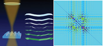
By combining standard through-the-lens viewing with a technique called scatterfield imaging, the NIST team accurately measured patterned features on a silicon wafer that were 30 times smaller than the wavelength of light (450 nanometers) used to examine them. They reported that measurements of the etched lines—as thin as 16 nanometers wide—on the SEMATECH-fabricated wafer were accurate to one nanometer.
credit: NIST/Barnes
(Recommended by Ed Perkins, posted by Yonhua Tzeng)
To read more:
- http://www.nist.gov/pml/div683/measuring_nanoscale_features_fractions_light_12-2-2015.cfm
- J. Qin, R.M. Silver, B.M. Barnes, H. Zhou, R.G. Dixson, and M.A.Henn,”Deep-subwavelength Nanometric Image Reconstruction using Fourier Domain Optical Normalization.” Light: Science & Applications. Article preview Nov. 5, 2015; e16038. To download: http://221.8.12.233/cms/accessory/files/AAP-lsa201638.pdf