IEEE NTC NANO BLOG


IEEE NTC Nano Blog is a platform for the world wide nanotechnology communities to share emerging and exciting progresses in research, development, commercialization, education, and opportunities related to nanotechnology. Recommendation of materials of significant impacts or common interest can be emailed to the Newsletter EiC, Jr-Hau (J.H.) He. For posting copyrighted materials in this website, permission from the copyright owner is necessary in advance. Names of persons recommending the posted materials will appear at the end of posts. EiC reserves the right to decide whether to post submitted materials in this website or not.
August 31, 2017 – Photon-triggered nanowire transistors are reported in Nature Nanotechnology
Kim et al., recently reported on photon-triggered nanowire (NW) transistors, a new step toward optical computing. These devices consist of crystalline silicon (CSi) NWs that include (PSi) segments in the middle and electrical contacts at both ends of the NW. The PSi acts as a reservoir and supplies carriers to the CSi channel when is exposed to light. It allows for an on/off ratio as high as 8×10⁶. Based on this method authors also demonstrated photon-triggered logic gates and a sub-micron resolution photodetector system.
![]()
To read more: https://www.nature.com/nnano/journal/vaop/ncurrent/full/nnano.2017.153.html
(Contents prepared by Dr. Noelia Vico Trivino and posted by Jr-Hau (JH) He)
A near-field cavity optomechanics readout concept has been integrated with picogram-scale probes to realize fully functional AFM detection. This allows achieving high temporal resolution (<10 ns) and picometer vertical displacement uncertainty simultaneously, breaking the trade-off between AFM measurement precision and ability to capture transient events.
Adapted with permission from Nano Lett., Article ASAP, DOI: 10.1021/acs.nanolett.7b02404. Copyright © 2017 American Chemical Society.
To read more: http://pubs.acs.org/doi/abs/10.1021/acs.nanolett.7b02404
(Contents prepared by Dr. Noelia Vico Trivino and posted by Jr-Hau (JH) He)
February 23, 2016 – Microtubules propelled by surface-adhered kinesin motors perform biocomputation
An international team of researchers has made a breakthrough in the field of biocomputation. By exploiting microtubules propelled by surface-adhered kinesin motors as motile nanoscale agents capable of performing basic computations, the subset sum problem was solved in a highly parallel approach. For more information, see Nicolau Jr. et al. in the Early Access Section of the Proceedings of the National Academy of Sciences:
To read more: http://www.pnas.org/content/early/2016/02/17/1510825113
(Contents prepared by H. Hess and posted by Y. Tzeng.)
December 25, 2015 – 2-D dichalcogenide MoS2 with PL QY of more than 95% is reported in Science
Amani et al. recently reported near-perfect two-dimensional transition metal dichalcogenide, MoS2 with photoluminescence quantum yield of more than 95% by chemical treatment in a nonoxidizing organic superacid: bis(trifluoromethane) sulfonimide (TFSI), which eliminates defect-mediated nonradiative recombination.
To read more: Near-unity photoluminescence quantum yield in MoS2. Matin Amani, Der-Hsien Lien, Daisuke Kiriya, Jun Xiao, Angelica Azcatl, Jiyoung Noh, Surabhi R. Madhvapathy, Rafik Addou, Santosh KC, Madan Dubey, Kyeongjae Cho, Robert M. Wallace, Si-Chen Lee, Jr-Hau He, Joel W. Ager III, Xiang Zhang, Eli Yablonovitch, Ali Javey. Science 27 November 2015: Vol. 350 no. 6264 pp. 1065-1068, DOI: 10.1126/science.aad2114
(Posted by Yonhua Tzeng)
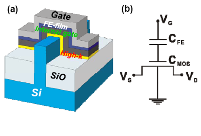
Negative Capacitance FET (NCFET) can be viewed as a FET with built-in voltage amplification. The first ALD ferroelectric HfZrO2 based negative-capacitance FinFET with gate length as small as 30 nm was reported in IEEE International Electron Devices Meeting (IEDM 2015) in Washington, DC USA. Small-signal voltage was amplified by 1.6X maximum at the internal gate with the sub-threshold swing improved from 87 to 55mV/decade. ION increased by >25% for the IOFF.
To read more: IEDM15-621 Paper #22.6.2
“Sub-60mV-Swing Negative-Capacitance FinFET without Hysteresis”
Kai-Shin Li(1), Pin-Guang Chen(2, 3), Tung-Yan Lai1, Chang-Hsien Lin(1), Cheng-Chih Cheng(3), Chun-Chi Chen(1), Yun-Jie Wei(1), Yun-Fang Hou(1), Ming-Han Liao(2), Min-Hung Lee(3), Min-Cheng Chen(1), Jia-Min Sheih(1), Wen-Kuan Yeh(1), Fu-Liang Yang(4), Sayeef Salahuddin(5), Chenming Hu(5)
(1) National Nano Device Laboratories, National Applied Research Laboratories, Hsinchu, Taiwan. (2) Department of Mechanical Engineering, National Taiwan University, Taipei, Taiwan. (3) Institute of Elecro-Optical Science and Technology, National Taiwan Normal University, Taipei, Taiwan. (4) Research Center for Applied Sci., Academia Sinica, Taipei,Taiwan. (5) Dept. of Electrical Eng. and Computer Science, University of California, Berkeley, USA; Tel: +886-3-572-6100 ext. 7706, Fax: +886-3-572-6109, Email: ksli@narlabs.org.tw
(Posted by Yonhua Tzeng)
December 14, 2015 – NIST Measured Nanoscale (16 nm) Features with Fractions of Light (450 nm)
By combining standard through-the-lens viewing with a technique called scatterfield imaging, the NIST team accurately measured patterned features on a silicon wafer that were 30 times smaller than the wavelength of light (450 nanometers) used to examine them. They reported that measurements of the etched lines—as thin as 16 nanometers wide—on the SEMATECH-fabricated wafer were accurate to one nanometer.
credit: NIST/Barnes
(Recommended by Ed Perkins, posted by Yonhua Tzeng)
To read more:
- http://www.nist.gov/pml/div683/measuring_nanoscale_features_fractions_light_12-2-2015.cfm
- J. Qin, R.M. Silver, B.M. Barnes, H. Zhou, R.G. Dixson, and M.A.Henn,”Deep-subwavelength Nanometric Image Reconstruction using Fourier Domain Optical Normalization.” Light: Science & Applications. Article preview Nov. 5, 2015; e16038. To download: http://221.8.12.233/cms/accessory/files/AAP-lsa201638.pdf
June 20, 2015 – Nano Modeling and Simulation – IEEE NTC Technical Committee
The Modeling and Simulation technical committee focuses on topics associated with the formulation, development and use of theoretical models for the understanding and design of nanotechnological systems for engineering applications in a wide spectrum of human society. For this purpose, it addresses technical issues related to the development of numerical codes requiring basic software as well as large-scale computational resources such as density functional theory, tight binding methods, self-consistent Poisson-Schrödinger solver, Monte Carlo simulation, non-equilibrium green function techniques, molecular dynamics to name a few. Among the current and latest topics of investigation are modeling of nanoscale electronic and photonic devices and systems, advanced devices made of new low-dimensionality materials such as graphene and transition metal dichalcogenides, spintronic devices and bio-nanoelectronic devices for molecular manipulation and sensing.
Schematic of a Graphene field effect membrane Transistor containing a nanopore for DNA sequencing (after
Anuj Girdhar, Chaitanya Sathe, Klaus Schulten and Jean-Pierre Leburton, PNAS, 110 (42) pp.1648-1653 (2013))
(Submitted by Jean-Pierre Leburton, posted by Yonhua Tzeng)
June 10, 2015 – NIST’s ‘Nano-Raspberries’ Could Bear Fruit in Fuel Cells
Researchers at the National Institute of Standards and Technology (NIST) have developed a fast, simple process for making platinum “nano-raspberries”—microscopic clusters of nanoscale particles of the precious metal. The berry-like shape is significant because it has a high surface area, which is helpful in the design of catalysts. Even better news for industrial chemists: the researchers figured out when and why the berry clusters clump into larger bunches of “nano-grapes.”
(Recommended by Ed Perkins, posted by Y. Tzeng)
May 9, 2015 – NIST-led Research Group Creates First Whispering Gallery for Graphene Electrons
Yue Zhao et al., an international team of scientists at the U.S. Commerce Department’s National Institute of Standards and Technology (NIST), demonstrated nanoscale whispering gallery electron resonance in graphene by using the probe voltage of a scanning tunneling microscope to create a circular pn junction in nanoscale area like a circular wall of mirrors to the electrons and similar to what happens to acoustic wave in the famous whispering gallery of St. Paul’s Cathedral.
“An electron that hits the step head-on can tunnel straight through it,” said NIST researcher Nikolai Zhitenev. “But if electrons hit it at an angle, their waves can be reflected and travel along the sides of the curved walls of the barrier until they began to interfere with one another, creating a nanoscale electronic whispering gallery mode.”
The potential of graphene-based quantum electronic resonators and lenses is believed to be huge.
Read the original press release and article: Center for Nanoscale Science and Technology/ NIST ; *Y. Zhao, J. Wyrick, F. Natterer, J. Rodriguez-Nieva, C. Lewandowski, K. Watanabe, T. Taniguchi, L. Levitov, N. Zhitenev, and J. Stroscio. Creating and probing electron whispering-gallery modes in graphene. Science. 8 May 2015: Vol. 348, no. 6235, pp. 672-675. DOI: 10.1126/science.aaa7469.

credit: Jon Wyrick, CNST/NIST
(Recommended by Ed Perkins, posted by Yonhua Tzeng)
May 8, 2015 – Pathway to the Piezoelectronic Transduction Logic Device
P. M. Solomon et al. proposed a piezoelectronic transistor (PET) not subject to the voltage limits of field-effect transistors. The PET transduces voltage to stress, activating a facile insulator−metal transition, thereby achieving multi-gigahertz switching speeds, as predicted by modeling, at low power. The team demonstrated a stress-based transduction principle. Read the original article: Nano Lett. 2015, 15, 2391−2395.
(Posted by Yonhua Tzeng. Adapted with permission from Nano Lett. 2015, 15, 2391−2395, DOI: 10.1021/nl5046796 Copyright © 2015 American Chemical Society.)
Huiliang Wang et al. demonstrated flexible CMOS-like logic circuits made of ambipolar single-wall carbon nanotube transistors fabricated without needing for doping processes using high-mobility electron-accepting (n-type) polymer sorted semiconducting SWCNT. Read the original article: Huiliang Wang et al., Adv. Funct. Mater. 2015, 25, 1837–1844. DOI: 10.1002/adfm.201404126 (Posted by Yonhua Tzeng)
May 7, 2015 – Majority logic gate for 3D nano-scale magnetic computing
Irina Eichwald et al. demonstrated the potential of 3D high integration density digital computing based on physically field interacting nanometer-scaled magnets with a bistable magnetization state, representing the Boolean logic states ‘0’ and ‘1’, arranged in a 3D manner. Read the original article: Irina Eichwald et al 2014 Nanotechnology 25 335202 doi:10.1088/0957-4484/25/33/335202
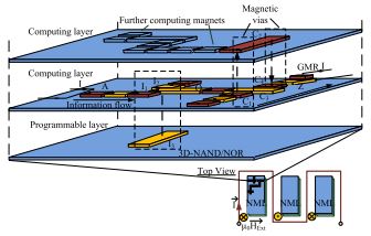
Schematic of a 3D NML logic system. Logic computing is performed by 3D NAND/NOR gates. Information between functional layers is transmitted by magnetic vias, enabling magnetic signal crossing and computing on a multi-level regime. Electrical in and output sensors enable us to transform magnetic information into the electrical domain and vice versa.
(Posted by Yonhua Tzeng)
May 4, 2015 – Wafer-Level Hysteresis-Free Resonant Carbon Nanotube Transistors
Wafer-level integration of resonant-body carbon nanotube (CNT) field-effect transistors (FETs) of >1M CNTFETs/cm2 with the resonance frequency tunable in situ by both a lateral gate and the back gate has been demonstrated by Ji Cao et al. offering promise in radio frequency signal processing and ultrasensitive sensing.
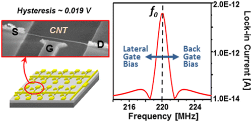
Adapted with permission from ACS Nano, 2015, 9 (3), pp 2836–2842 DOI: 10.1021/nn506817y. Copyright © 2015 American Chemical Society. (Posted by Yonhua Tzeng)
Zheng et al. demonstrated Ge-MOSFET with negligible C−V hysteresis, extremely low leakage, and superior equivalent oxide thickness by the aid of a fluorinated epitaxial graphene on Ge as an oxygen diffusion barrier to successfully prevent the formation of unstable germanium oxide between the Ge channel and the HfO2 gate oxide. Read the original article: Xiaohu Zheng et al., Adv. Funct. Mater. 2015, 25, 1805–1813 (Posted by Yonhua Tzeng)
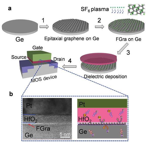
a) Schematic diagram showing the implementation of FGra as the diffusion barrier layer between the Ge substrate and HfO 2 dielectric layer in the Ge-based MOS device: (step 1) direct growth of continuous monolayer graphene on Ge; (step 2) FGra synthesized by exposure to SF 6 plasma; (step 3) dielectric deposition on FGra/Ge by atomic layer deposition; (step 4) MOS device completed by standard semiconductor manufacturing processes. b) Cross-sectional high-resolution TEM of the gate stack showing the absence of interfacial oxide formation in the presence of FGra and schematic diagram showing retarded diffusion in the vicinity of high- k /Ge interface. (Credit Xiaohu Zheng et al., Adv. Funct. Mater. 2015, 25, 1805–1813 with permission)
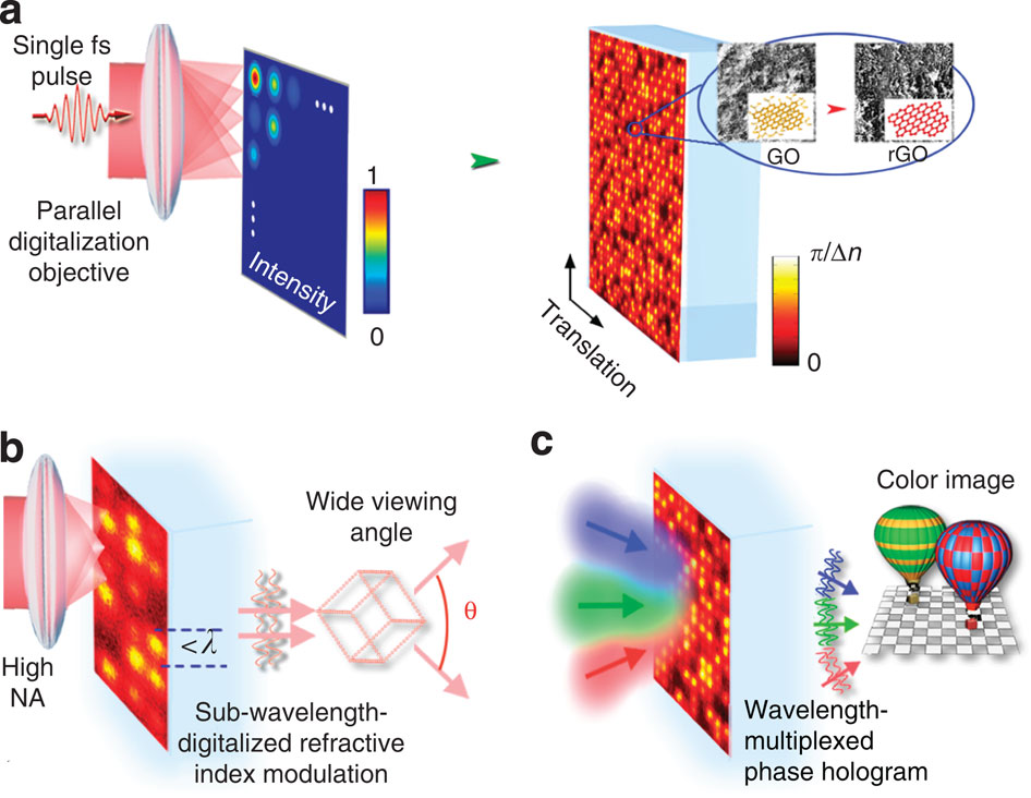
April 29, 2015 – Subwavelength-scale Photoreduced Graphene Oxides Enable Holographic Images
Xiangping Li et al. demonstrated write-once holograms for wide-angle and full-colour three-dimensional images using subwavelength-scale pulsed femtosecond laser reduction of graphene oxide to enable multilevel optical index modulation and restoration of vectorial wavefronts of polarization discernible images through the vectorial diffraction of a reconstruction beam. Read the original article: Li et al., Nature Communication (2015) (Posted by Y. Tzeng)
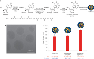
Alice Gaudin et al. used squalenoyl adenosine nanoparticles of the size of ∼120 nm as a neuroprotective drug to deliver therapeutic amounts of drugs by intravenous injection for treating nervous system after stroke and spinal cord injury of mice. Read the original article: Nature Nanotechnology, doi:10.1038/nnano.2014.274 (Posted by Y. Tzeng)
Te-Fu Yeh et al. of National Cheng Kung University in Tainan, Taiwan invented nitrogen-doped graphene oxide quantum dots containing p-n type photochemical diodes, which catalyze water-splitting under visible-light irradiation mimicking biological photosynthesis. Read the original article and report: Advanced Materials doi/10.1002/adma.201305299, NCKU Research Express
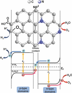
(Upper) Nitrogen-doped graphene oxide quantum dots. (Lower) quantum dot p-n diode for water splitting. Credit : Te-Fu Yeh et al., Advanced Materials (Posted by Y. Tzeng)
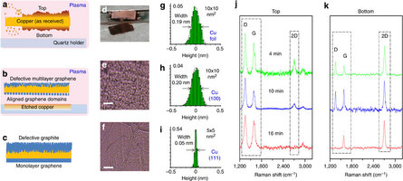
April 26, 2015 – Low-temperature PECVD of High-mobility Graphene on Copper Foils
Boyd et al. of California Institute of Technology demonstrated a microwave plasma-enhanced CVD chemistry in gas mixtures of hydrogen, methane, and nitrogen that grows graphene on copper foils at temperatures lower than 420 °C exhibiting sub-nanometer smoothness, excellent crystalline quality, low strain, few defects and room-temperature electron mobility up to (6.0±1.0) × 10000 cm2 V−1 s−1. Read the original article: NATURE COMMUNICATIONS doi:10.1038/ncomms7620 ( Posted by Y. Tzeng)
April 23, 2015 – Coaxial Lithography with Sub-10 nm Architectural Control
Tuncay Ozel et al. of Northwestern University demonstrated a core/shell semiconductor nanowire with an embedded plasmonic nanoring, which could not be fabricated by any previously known method, using templated electrochemical synthesis termed as coaxial lithography. Read the original article: Nature Nanotechnology doi:10.1038/nnano.2015.33 (Posted by Y. Tzeng)
Kolkowitz et al. of Harvard University used nitrogen-vacancy centers in diamond to make single-spin qubits for measuring Johnson noise thermally induced in a conductive silver film in the vicinity indicating that nanoscale quantum systems may be controlled by nearby electrodes. Read the original article: Thermally induced electrical currents, known as Johnson noise, cause fluctuating electric and magnetic fields in proximity to a conductor. These fluctuations are intrinsically related to the conductivity of the metal. We use single-spin qubits associated with nitrogen-vacancy centers in diamond to probe Johnson noise in the vicinity of conductive silver films. Measurements of polycrystalline silver films over a range of distances (20 to 200 nanometers) and temperatures (10 to 300 kelvin) are consistent with the classically expected behavior of the magnetic fluctuations. However, we find that Johnson noise is markedly suppressed next to single-crystal films, indicative of a substantial deviation from Ohm’s law at length scales below the electron mean free path. Our results are consistent with a generalized model that accounts for the ballistic motion of electrons in the metal, indicating that under the appropriate conditions, nearby electrodes may be used for controlling nanoscale optoelectronic, atomic, and solid-state quantum systems. Science 6 March 2015: Vol. 347 no. 6226 pp. 1129-1132, DOI: 10.1126/science.aaa4298 (Posted by Y. Tzeng)
April 23, 2015 – All-electric all-semiconductor spin field-effect transistors
Pojen Chuang et al. of National Cheng Kung University in Tainan, Taiwan and his co-workers used two quantum point contacts as spin injectors and detectors to achieve complete control of the electron spins (spin injection, manipulation and detection) in a purely electrical all-semiconductor spin field-effect transistor which is compatible with large-scale integration and promising for future spintronics based information processing. Read the original article: Pojen Chuang, Sheng-Chin Ho, L. W. Smith, F. Sfigakis, M. Pepper, Chin-Hung Chen , Ju-Chun Fan , J. P. Griffiths, I. Farrer, H. E. Beere, G. A. C. Jones, D. A. Ritchie and Tse-Ming Chen. All-electric all-semiconductor spin field-effect transistors. Nature Nanotechnology DOI: 10.1038/NNANO.2014.296 (Posted by Y. Tzeng)

April 22, 2015 – Low Energy Loss Cold Electron Transport in Devices Operating at Room Temperature
Professor Koh and his team at University of Texas at Arlington reported in Nature Communication a means of enabling electrons to transport at room temperature like electrons do at very low temperatures with little energy loss by passing electrons through an energy filter made of a quantum well. The team has received funding to apply the discovery to high-density transistors made in the form of nanopillars. Read the original reports: Nanotechnology aids in cooling electrons without external sources, Energy-filtered cold electron transport at room temperature.
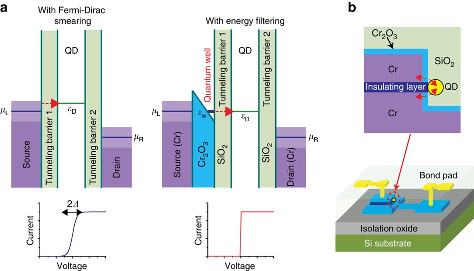
(a) Left: the double-barrier tunnel junction (DBTJ) structure. (a) Right: DBTJ structure with a quantum well inserted between the source and tunnelling barrier 1. (b) Schematic of the DBTJ structure with the energy filter inserted. Top: cross-sectional view. The dotted arrows indicate electron tunnelling paths. Bottom: three-dimensional view of one device unit. The schematics are not to scale. Credit Koh et al., Nature Communication. (Posted by Y. Tzeng)
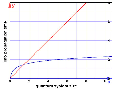
April 14, 2015 – NIST Tightens the Bounds on the Quantum Information ‘Speed Limit’
NIST scientists prove that the propagation time of entanglement between two distant particles for sharing data across a quantum system grows only as a power of the system size instead of logarithmically. The finding implies that quantum processors will be slower than previously predicted. (Posted by Ed. Perkins, Y. Tzeng)
December 16, 2014 – NIST Sensor Enables Self-calibrating AFM
Pressure of light from an optical fiber sets an AFM tip vibrating, of which the movement is measured by an interferometer through another optical fiber giving a value of the probe ‘s stiffness as a means of self-calibration. (Posted by Ed Perkins, Y. Tzeng)