IEEE Nanotechnology Council
Advancing Nanotech for Humanity
IEEE

Archive for the ‘Technical Activities’ Category

IEEE NTC Shanghai Chapter 2023-2024 Nanotechnology Distinguished Seminars

Wednesday, April 24th, 2024

From December 2023 to January 2024, Nanotechnology Distinguished Seminars (NDS) were held three times in the IEEE Nanotechnology Council (NTC) Shanghai Chapter, China. NDS Series are proposed and chaired by Prof. Weida Hu from the Shanghai Institute of Technical Physics (SITP) as the Chair of IEEE NTC Shanghai Chapter with Prof. Ivan Iorsh from lTMO University, Prof. Mario Lanza from the King Abdullah University of Science and Technology and Prof. Wenwu Pan from the University of Western Australia. There were totally 48 participants coming from China, Russia, and Saudi Arabia. NDS Series invited experts with various backgrounds to bring cutting-edge nanotechnology knowledge to our students, break down information barriers, and ultimately achieve collaborative development within the organization. A series of insightful presentations showcased groundbreaking developments in nanotechnology. Highlights of the talks included:

• Combining two-dimensional semiconductors with metasurfaces
• Hybrid 2D/CMOS microchips
• Dislocation Filtering Technology for defect reduction on heteroepitaxially-grown semiconductors

Prof. Ivan Iorsh from lTMO University briefly reviewed their recent results on the light-matter coupling in 2D semiconductors integrated with photonic nanostructures. He also discussed how the realization of strong light-matter coupling might facilitate the suppression of the inhomogeneous broadening of excitons and induce a strong nonlinear optical response. Furthermore, He showed how the excitonic properties can be controlled via strong light-matter coupling and finally discussed how one can exploit strong magnetic proximity effect in order to enable magnetooptics with 2D materials.

Prof. Mario Lanza from the King Abdullah University of Science and Technology discussed how to integrate 2D materials in micro/nano-electronic devices, circuits, and microchips, giving a general overview of the global progress achieved in the field and presenting our last developments in hybrid 2D/CMOS applications. He put special emphasis on devices and circuits for memristive technologies, including data storage, computation, encryption, and communication. He also discussed the main technological challenges to face in the next years and provided some recommendations on how to solve them.

Prof. Wenwu Pan from the University of Western Australia showed the use of strained CdZnTe/CdTe superlattice layers as dislocation filter layers for the heteroepitaxy of II-VI CdTe buffer layers on lattice-mismatched III-V GaAs substrates. Their experimental results reviewed here suggest that the dislocation filtering technology is a promising approach for achieving high-quality heteroepitaxy of semiconductors on large-area lattice-mismatched substrates, which is crucial for the fabrication of high-performance optoelectronic devices, especially monolithically integrated devices.

The IEEE NTC Shanghai Chapter Nanotechnology Distinguished Seminar Series was a great success, making all participants rejoice in their contribution to the synergistic development within IEEE NTC Shanghai Chapter and future endeavors in the field of nanotechnology.


TC 16: Update on Upcoming and Past Activities

Saturday, April 20th, 2024

Update on Upcoming and Past Activities

  1. Ising Machine Workshop (IISM) 2024
    The International Workshop on Ising Machines (IISM) 2024 took place in Messina, Italy from April 16 to 18, 2024. You can explore the comprehensive coverage of topics discussed, including theoretical insights into Ising machines, digital applications, simulations of innovative computing paradigms, and advancements in analog and hybrid Ising machines here.
  2. Virtual Workshop on “Next Generation Computing in the Era of Chiplets”
    On February 29, 2024, a virtual workshop was held focusing on the paradigm-shifting concept of Chiplets and their integration potential with semiconductor and emerging technologies. Discover more about this workshop here.
  3. Roadmap for Emerging Technologies-based Unconventional Computing
    Delve into a perspective paper on the utilization of emerging technologies like photonics, superconducting materials, and spintronics for unconventional computing paradigms such as neuromorphic and quantum computing. Read the publication here.
  4. Special Issue on “Neuromorphic Computing”
    We initiated a special issue on “Neuromorphic Computing” in the IEEE Transactions on Nanotechnology. For more information, visit here. The submission deadline was September 30, 2021.
  5. Second Meeting of TC-16 on Quantum, Neuromorphic, and Unconventional Computing
    The virtual workshop on unconventional computing with emerging technologies was held on May 13, 2022. Explore the workshop’s schedule, recording, and talks here. Additionally, you can access the talks on YouTube here.
  6. Kickoff Meeting of TC-16 on Quantum, Neuromorphic, and Unconventional Computing
    The inaugural meeting was held on June 11th, 2021. Access the meeting’s schedule, recording, and talks here. Talks are also available on YouTube here.

IEEE NTC Volunteer Summer Internship Program

Saturday, December 9th, 2023

The IEEE Nanotechnology Council (NTC) is committed to offering opportunities for motivated high school students in the U.S. to engage in immersive and comprehensive learning experiences. Through their Volunteer Summer Internship Program, the NTC connects students with technology professionals from various organizations, fostering education and innovation.

Mission: The mission of the IEEE NTC Volunteer Summer Internship Program is to provide high school students in the U.S. with opportunities in modeling and simulation, literature review and technical writing. This is achieved by connecting them with industry experts, educators, and mentors, preparing them intellectually and emotionally for their future endeavors.

Vision: The vision of the program is to bring appropriate opportunities to interested high school students. These opportunities allow students to interact with experts in industry and academia.  The program aims to provide students with valuable experiences related to nanotechnology. .

Summer Internship Program

As part of its commitment to fostering education and innovation, IEEE NTC offers a Summer Internship program in collaboration with Eastern Washington University (EWU) and the University of Washington (UW). This program provides high school students with the opportunity to engage in hands-on research in various areas, including 2D Materials, Neuromorphic Computing, and Technical Writing.

The program  allows mentors to work directly with highly dedicated students who demonstrate a strong understanding of the concepts. Under the guidance of mentors from academia and industry, students explore the applications and science behind nanomaterials, quantum dots, and neural networks. 

Arpan De shares his experience as a mentor, highlighting the benefits of learning topics at a grassroots level and developing time management skills. The program also allows mentors to work with highly dedicated students who demonstrate a strong understanding of the concepts. The remote internship lasts for six or more weeks between June and August, providing aspiring young scientists with a valuable learning experience. 

Get Involved

If you are interested in mentoring students in the Summer Internship program or require further information, please reach out to M. P. Anantram at anantmp@uw.edu or Arindam Kumar Das at arindam@uw.edu. High school students can apply for the Summer Internship program in late February 2024 at the SPARK SIP website.

Alternative Careers for Nanotechnology Researchers

Saturday, December 9th, 2023

Recent PhD graduates in the field of nanotechnology have a wide range of career options to consider. This article will explore some of the exciting career paths available in this field, other than conventional roles of postdoctoral fellow in academia or research scientist in industry.

Representative Image by Eddie Mar Delos Angeles from Pixabay

1. Product Development Engineer

In this role, you will apply your expertise in nanotechnology to develop innovative products and materials. You will work closely with design and manufacturing teams to optimize product performance and functionality. Your simulations will guide the development process, ensuring that the final product meets desired specifications. Additionally, you will stay updated with the latest advancements in nanoscale modeling to continually improve product designs.

2. Computational Scientist

As a computational scientist specializing in nanotechnology modeling and simulation, you will develop and optimize simulation algorithms and techniques. Your expertise will enable you to tackle complex problems in nanoscience and nanotechnology, advancing our understanding of nanoscale phenomena. You may collaborate with other researchers and industry professionals to solve real-world challenges and drive technological innovations.

3. Entrepreneur

With a strong background in nanotechnology, you have the potential to start your own venture in this field. You can explore opportunities to develop simulation software, build a semiconductor foundry, provide consulting services, or create innovative solutions for specific industries. As an entrepreneur, you will have the freedom to pursue your own ideas and make a significant impact in the nanotechnology sector.

4. Patent Attorney

As a patent attorney specializing in nanotechnology, you can help protect intellectual property and navigate the legal aspects of inventions and innovations in this field. Your expertise in nanotechnology will be valuable in understanding the technical aspects of patents and providing guidance to inventors and companies seeking patent protection.

5. Technology Transfer Officer

In this role, you will bridge the gap between academia and industry by facilitating the transfer of nanotechnology research and technology to commercial applications. You will work with researchers, industry partners, and legal professionals to identify market opportunities, negotiate licensing agreements, and support the commercialization of nanotechnology innovations.

6. Policy Advisor

As a policy advisor in the field of nanotechnology, you will have the opportunity to influence and shape regulations and policies related to nanoscale technologies. Your expertise in nanotechnology will provide valuable insights into the potential risks and benefits of these technologies. You will work with government agencies, industry stakeholders, and scientific communities to develop policies that promote responsible and sustainable development of nanotechnology.

The field of nanotechnology offers a wide range of exciting career options for recent PhD graduates in nanoscale modeling and device development. With your contributions, you can advance scientific knowledge, drive technological innovations, and shape the future of nanotechnology. The possibilities are endless in this rapidly evolving field.

By embracing collaboration, we can push the boundaries of scientific understanding and continuously explore the endless possibilities that nanotechnology has to offer.

Best of luck in your career in nanotechnology!

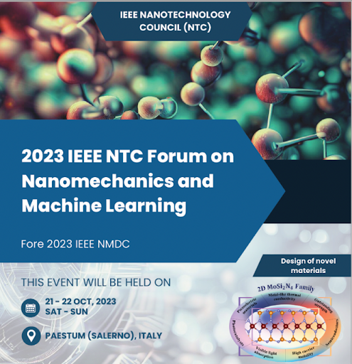
NTC Forum on Nanomechanics and Machine Learning

Thursday, December 7th, 2023


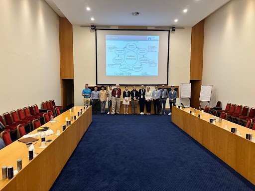
Before the IEEE NMDC 2023 Conference (23-25 Oct. 2023), the NTC focus forum on Artificial Intelligence (AI) and Nanotechnology was held in Mercurio Hall in Ariston Hotel, Paestum, on 21-22 Oct. 2023. The forum is proposed and Chaired by Prof. Dr. Xiaoying Zhuang from Leibniz University Hannover, Germany, with Prof. Xiaoning Jiang from NC State representing NTC as the VP TA. Dr. Teresa Cheng from Leibniz University Hannover and Dr. Quanzhou Yao from South China University of Science and Technology helped with the organization. There were totally 12 participants coming from Australia, Belgium, China, Germany, Norway, Switzerland and the US including Mr. Tylor Jaynes from the NTC Standards Committee who participated as an additional observer. The forum invited experts with various background including AI algorithm, metamaterials, nanomechanics experiments, nano tribology, nanomaterials design, nanomaterials manufacturing, packaging, nano energy harvesters, photodetectors, 2D materials etc in order to bring chemistry of new ideas and explore new ideas of AI in nanotechnology. Enhancing our interactive session, one of our attendees contributed to the discussions via an online connection. A series of twelve insightful presentations showcased groundbreaking developments in AI as applied to the field of nanotechnology. Highlights of the talks included:

• AI enhanced energy harvester design and applications;
• AI assisted experiment on mechanical characterization, such as piezoelectric thin film and high entropy alloys;
• AI assisted inverse design of metamaterials
• AI assisted 2D materials characterization;
• AI assisted experimental results, such as piezoresponse force microscopy (PFM) for accelerated potential valley of stick-slip behaviour in tribology, and for high quality PFM images;
• AI based nano materials design and exploration;

The forum also discussed the issues regarding the AI applications in nanotechnology, including the demand of a large number of data and the physics issues that gives “sense” to the results or output from AI. Research related to “AI and Nanotechnology” showed interesting potential and a pre-forum study made by Prof. Zhuang showed that AI is among the most active and rising directions in nano materials and nano technology around the world where many interesting examples have revealed the perspectives. Dr. Jakob Schwiedrzik from EMPA at Switzerland presented extreme naonmechanics testing with self-developed instruments at EMPA of extremely high strain rate testing as well as cryogenic and high temperature. He also showed AI based data analysis of large datasets generated by high throughput multimodal materials characterization for various applications. Prof. Jim Morris from Portland State University gave an overview talk of NTC history and future perspective and afterwards he presented issues and uncertainties in electric conduction of discontinuous metal nanoparticle in thin film. Prof. Jianying He presented additively manufactured high entropy alloys where AI can be used to accelerate and optimize the manufacturing parameters for high strength alloy. Prof. Yabin Jin from Tongji University showed the AI enhanced inverse design of metamaterials and topological insulating structures where AI can accelerate novel functions and features. Prof. Timon Rabczuk from Bauhaus University Weimar presented AI mathematical model, theory and algorithms for scientific computing and materials design. He also showed the insight of Dr. Binh Huy Nguyen from Interuniversity Microelectronics Centre (imec), Belgium presented AI assisted MEMS design and characterization. Prof. Di Bartolomeo presented interesting findings of photoconductivity, negative photoconductivity and pressure hysteresis of several 2D materials including MoS2 and ReS2 etc. Prof. Xiaoying Zhuang presented the AI based 2D materials exploration and multiscale materials characterization and homogenization using deep learning. Dr. Quanzhou Yao from South China University of Science and Technology presented AI enhanced solution of for the statistical study of stick-slip events in nano triboelectricity. Dr. Qiong Liu demonstrated recent results on PFM and Ramen spectrum characterization of flexoelectricity of 2D materials. Dr. Teresa Cheng summarize the state of the art of nano energy harvesters and future perspective about how to use AI to develop more efficient energy harvester.

During the forum, several discussion sessions were carried out and it was agreed that it is important to disseminate and demonstrate successful showcases to NTC and IEEE community where AI can be used to enhance current research methods. It was proposed that it is necessary to organize and provide training courses or lectures that can deliver basic mathematical models and knowledge of using AI. Issues of data generation raised a lot of discussions and questions regarding the quality and quantitates of the data. A key step is of course to see the problem for each researcher that can be improved or solved by AI. Future plans under consideration are the foundation of new technical committee within NTC in the area of “AI and Nanotechnology”, special sessions in IEEE Nano 2024 in Spain and the further communications with other IEEE societies such as Computer Science. A special issue of NTC journals or the magazine is under discussion and envisioned to be organized.


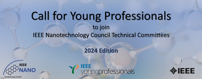
Call for Young Professionals to Join IEEE Nanotechnology Council Technical Committees

Saturday, December 2nd, 2023

Third Call for Young Professionals to Join IEEE Nanotechnology Council Technical Committees

Are you interested in the field of Nanotechnology and in expanding your professional horizons? Consider joining one of the IEEE Nanotechnology Council Technical Committees. Our mentoring program (MENED) is designed for young professionals interested in gaining new skills and experiences, participating in professional activities, and further development of their professional network.

The major strength of IEEE Nanotechnology Council (NTC) resides in its large number of members and volunteers, and the unlimited spectrum of nanotechnology applications. Currently, the IEEE NTC activities (technical, educational, conferences, publications, standing committees, etc.) and initiatives are extremely rich and rise the IEEE NTC to the level of a well-recognized world leader in the field of nanotechnology. To guarantee sustainability of NTC activities and to enable successful succession planning in the NTC’s leadership, an initiative was launched at the beginning of 2022, namely the IEEE NTC Mentoring program: from Effectiveness to Durability, or the so-called NTC MENED program. The NTC MENED program aims to enable the NTC volunteers to grow indispensable skills to carry out the NTC activities and to gradually integrate a larger number of well-trained NTC volunteers into the different initiatives. The objectives of NTC MENED program are as follows: 1) To reach a high level of success in the NTC activities; 2) To maximize the chance of new volunteers to reach their goals; and 3) To establish a mentoring culture that concerns the durability of NTC MENED program. Through the NTC MENED program, the final goal of NTC is to connect people and create teams in which everyone brings ideas, trust and rapport.

Find your chosen technical committee and fill out our short application form so we can get to know you better. Deadline is JANUARY 15, 2024.


2023 IEEE NTC TC10 Modeling and Simulation December Webinar

Tuesday, November 14th, 2023


Webinar 3

Date: December 12, 2023
Time: 1600-1700 CET (GMT+1)

Speaker: Dr. Tue Gunst,

Organizer: Josef Weinbub, TC 10 Co-Chair, weinbub@iue.tuwien.ac.at

Topic: QuantumATK: Interfacing cutting-edge practical nanoelectronic applications with advanced atomistic simulations

View recording here.

Abstract:

Advancing next-generation nanoelectronics requires integrating atomistic cutting-edge simulation methods into realistic nanoelectronic device models. In this webinar, I will demonstrate how machine-learned force fields and multi-model simulators can be used to model nanoelectronic research problems by combining realistic interfaces, flexible electrostatic solvers, and advanced transport analysis. I will also highlight the latest trends in QuantumATK modeling and present case studies relevant to the nanoelectronic industry.

Presenter:

Tue Gunst is a senior application engineer at Synopsys working on advanced transport and materials applications in the QuantumATK team. Tue specializes in  nanoelectronics modeling, using his background as a university scientist (Post Doc & assistant professor at the Technical University of Denmark from 2013 to 2019) to bridge the gap between the newest simulation methodologies and applications relevant to key industry players. Tue collaborated closely with QuantumATK teams throughout his university research projects and joined Synopsys in 2019 to accelerate the utilization of advanced modeling techniques in nanoelectronic research applications.


Registration for meeting link (closed)


Quantum Technologies: Pathways Beyond Classical Systems Workshop

Wednesday, October 18th, 2023

Quantum Technologies: Pathways Beyond Classical Systems Workshop


Location & Time: Utah Valley University, CS 404 (800 W University Pkwy, Orem, UT 84058 USA), 1 – 5 pm MST [UTC -7], November 10, 2023

This high-level workshop aims to provide an overview of the current efforts to organize quantum-related academic, industrial, and professional activities in:
– Computer science
– Electrical and electronics engineering,
– Industrial standards development,
– Information science (including information technology management),
– Network architecture and infrastructure development, and
– Sustainability by design.

In person or virtual participation is open to all members of the public. Please register using this form: https://forms.gle/f4bmPRDie8g1BHAW9

Tentative agenda (official agenda to be mailed the week of the event):

13:00 – 13:50, Session 1 – Developing Technical Communities for Quantum Electrical Engineering (QEE) and Quantum Information Technology (QIT)
14:00 – 14:50, Session 2 – Roadmaps for QEE and QIT, and the Need for Ethically-Aligned Design (EAD)
15:00 – 15:50, Session 3 – Quantum Computer Architecture and Standardization
16:00 – 17:00 – Time allotted for networking and local community organizing

Sixth Meeting of the NTC Technical Committee on Emerging Plasma Nanotechnologies

Friday, October 6th, 2023

The Technical Committee on Emerging Plasma Nanotechnologies of the IEEE Nanotechnology Council plans to hold its sixth online workshop Tuesday October 17th, at 10:00 am EST, US Eastern time zone. The theme we are targeting is plasma-surface measurements and modeling (graphene, BN…) related but not limited to emerging device and sensor applications.

We have two distinguished speakers, Yevgeny Raitses from Princeton Plasma Physics Laboratory and Roberto Longo from Tokyo Electron America, Inc. With this line-up we cover the gamut of experiment and simulation related to nanomaterial formation.

The talks are intended to be 30 min in length with 5 min for questions.

The agenda follows:

10:00-10:05 am EST Welcome
10:05-10:40 am EST Yevgeny Raitses  – Plasma-based technologies for synthesis and processing of carbon and boron nitride nanomaterials
10:40-11:15 am EST Roberto Longo – Mechanisms for Graphene Growth on SiO2 using Plasma Enhanced Chemical Vapor Deposition

Start times in other time zones are:

New York (USA – New York) Tuesday, October 17, 2023 at 10:00:00 am EDT UTC-4 hours
Austin (USA – Texas) Tuesday, October 17, 2023 at 9:00:00 am CDT UTC-5 hours
London (United Kingdom) Tuesday, October 17, 2023 at 3:00:00 pm BST UTC+1 hour
Tokyo (Japan) Tuesday, October 17, 2023 at 11:00:00 pm JST UTC+9 hours


Organizers:

Dr. Peter Ventzek

Prof. Uros Cvelbar

Dr. Kremena Makasheva

Committee Chair: Prof. Seiji Samukawa

Members of TC17 Emerging Plasma Nanotechnologies Technical Committee, IEEE Nanotechnology Council


We invite you to attend. Attendance is free but registration is necessary.

Use this form to register:


    NTC TC17 Sixth Online Workshop Meeting Registration (free)

    Your name

    Your email

    You will receive the meeting invitation in email

    I accept the IEEE Terms and Conditions and the IEEE Privacy Policy.

    Please note while it may seem the form is waiting after submit, the message has been sent, so you can leave this page after a few seconds.

    2023 IEEE NTC TC10 Modeling and Simulation October Webinar

    Friday, August 4th, 2023

    IEEE Nanotechnology Council TC10 – Modeling and Simulation 2023 webinar series.

    Organizer: Josef Weinbub, TC 10 Vice Chair, weinbub@iue.tuwien.ac.at
    Format: 1 hour Webex webinars

    Webinar 2

    Date: October 12, 2023
    Time: 16:00 PDT, 1:00 CEST, 08:00 JST

    Speaker: Gerhard Klimeck, Professor and nanoHUB Director, Purdue University

    Topic: nanoHUB for Research and Education in Nanoelectronics

    Register below to receive meeting link

    Abstract

    Over 200,000 nanoHUB users have run over 7 million simulations in Apps mostly focused on semiconductor devices and materials modeling. These apps provide very simple and intuitive interfaces to community and research codes that are hard to install, operate, and to maintain even for experts.   As such nanoHUB created the first end-to-end scientific cloud enabling users to focus on solving problems rather than installing and maintaining software (before “the cloud” was a thing).  Any portal provides access, installation, and compute cycles, however, usability is most often neglected.  Most scientific tools focus on solving “any” simulation problem in a specific problem range.  Such comprehensiveness makes these tools usable by experts only, typically after intensive training.  nanoHUB has instead focused on delivering a spectrum of apps that individually have a limited capability compared to the underlying toolset, but as a whole set cover a vast swath of problems. Hundreds of community members have contributed over 700 Apps into nanoHUB.

    We assembled some of these Apps that are essential for specific courses into small sets such as ABACUS (crystals, bandstructure, drift-diffusion, pn-junctions, BJTs, MOScaps, MOSFETs) [1].  The usability results are stunning.  Our user analytics prove that over half of the simulation users participate in structured education through homework/project assignments.   We can identify classroom sizes and detailed tool usage [2,3]. We can begin to build mind-maps of design explorations and assess depth of explorations for individuals and classes. While parts of academia struggled to innovate curricula, we have measured the median first-time App insertion into a class to be less than six months.  Over 180 institutions have utilized nanoHUB in their curriculum innovation in over 3,600 classes.   2 million nanoHUB visitors explore lectures and tutorials annually.  Over 2,700 papers cite nanoHUB in the scientific literature resulting in 68,300+ secondary citations and an equivalent h-index of 121.

    With such a community presence we believe nanoHUB is the platform of choice to deliver online modeling, simulation, virtual environments, and lectures for the US initiative on workforce development and chip design [4]. We are in the process to build chipshub.org as a group inside nanoHUB.  Chipshub hosts commercial and open-source chip design tools and associated apps and learning materials.   It is hosted in Purdue’s hardware cloud.

    [1] https://nanohub.org/groups/abacus ABACUS – Assembly of Basic Applications for Coordinated Understanding of Semiconductors.  A one-stop-shop for teaching and learning semiconductor fundamentals.

    [2] Krishna Madhavan, Michael Zentner, Gerhard Klimeck, “Learning and research in the cloud”, Nature Nanotechnology 8, 786–789 (2013)

    [3] TEDx Talk, Klimeck, “Mythbusting Scientific Knowledge Transfer with nanoHUB.org”, https://www.youtube.com/watch?v=PK2GztIfJY4 .

    [4] https://chipshub.org

    Speaker:

    Dr. Gerhard Klimeck is a Professor of Electrical and Computer Engineering at Purdue University; Director of the Network for Computational Nanotechnology; Reilly Director of the Center for Predictive Materials and Devices. He helped to create nanoHUB.org, the largest virtual nanotechnology user facility serving over 2.0 million global users, annually. Dr. Klimeck is a fellow of the Institute of Physics (IOP), the American Physical Society (APS), the Institute of Electrical and Electronics Engineers (IEEE), the American Association for the Advancement of Science (AAAS), and the German Humboldt Foundation. He has published over 525 printed scientific articles; he has been recognized for his co-invention of a single-atom transistor, quantum mechanical modeling theory, and simulation tools. His NEMO5 software has been used since 2015 at Intel to design nano-scaled design transistors. The nanoHUB team was recently recognized by a top 100 by R&D award – Making simulation and data pervasive.


    Register for meeting link:

      2023 IEEE NTC Modeling and Simulation Webinar Series

      Webinar 3 December 12 Registration (free)

      Your name

      Your email

      You will receive the meeting invitation in email

      I accept the IEEE Terms and Conditions and the IEEE Privacy Policy.

      Please note while it may seem the form is waiting after submit, the message has been sent, so you can leave this page after a few seconds.