San Francisco Bay Area Nanotechnology Council Chapter hits the mark with 3 Day nanotechnology workshop for Students.
By Nick Massetti IEEE Life Senior Member
I’ll tell the story of the event titled: IEEEnanoCON-2016: Inspiring the Next Generation by starting at the end.
Slides of selected presentations of the IEEE SFBA Nanotechnology Council Chapter 3-Day Workshop on Nanotechnology can be found at the following link: https://goo.gl/HbKoD8
The following are some of the comments from attendees following the 3 day mid-year workshop on nanotechnology designed for college students on Summer break and young professionals.
“First and foremost, I’d like to say that I enjoyed almost every single aspect of the event, and in particular, I thought the diversity of speakers (especially the balance between industry and academia) and locations was excellent.” Alex, UC Davis Chem E. undergrad.
“In my experience, the three days of IEEEnanoCON-2016 resulted in a fantastic combination of getting up to speed in areas of my own interest (biotechnology and medical devices) and developing knowledge and ideas in new polymers, new semiconductor materials, addressing energy needs and clean technologies. To make all this possible, the program brought together an excellent panel of presenters from industry, academia and government research to interact with a very enthusiastic and curious group of young scientists and engineers, from elite schools, universities and colleges from all over. I take away the inspiration and the energy of a new generation of scientists to lead the field in decades to come.” Maria, Ph.D., EMBA, Medical Device Consultant
“I am deeply grateful for the education I have received from the three days of incredible speakers, great itineraries, enjoyable food, and excellent networking. This event has helped me see possibilities for myself that hadn’t occurred to me before.” Margaret, Undergrad, Foothill College.
The inspiration for the event grew from the RFP issued by the IEEE NTC in early 2015 for a Summer School on Nanotechnology. Although the San Francisco Chapter’s proposal was not the proposal selected for funding, the organizers moved ahead and found local sponsors to subsidize student registration fees and some other event costs. The workshop presented leading industrial scientists, academic researchers, entrepreneurs and government speakers in a broad spectrum of nanotechnology topics. The event was held at three separate locations, one day at each location. Part of the concept involved inviting researchers and interns at the different sites to attend providing golden network opportunities for the registrants. It also provided an opportunity for the registrants to go on tours of the local labs, for example, the Stanford University Nanofabrication Facility.
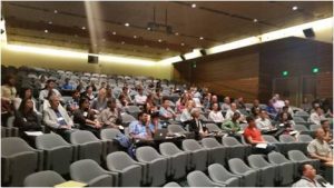
When the attendance numbers were totaled the student participation alone reached 59 including nine Texas Instruments student interns, who dropped in on day one, and ten IBM student interns, who participated on day two. In addition to local interns there were also seasoned researchers and professors who stopped in for presentations and some even helped the speakers answer questions. The students reported attending at least 18 universities across the USA and the UK during the academic year. Besides the USA, home countries included Canada, India, Iran, Japan, Russia, and Vietnam. Many were interning at local industrial companies such as Semiconductor equipment supplier Applied Materials, biopharma giant Gilead, Zeiss X-Ray and research giant XEROX-PARC. Event sponsors included IBM, SWCNT manufacturer OCSiAl LLC, and the IEEE SCV Section STEM education fund.
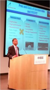
The talks were led off by IEEE NTC Pioneer and NASA Chief Scientist Dr. Meyya Meyyappan, shown here, who described carbon nanotube based sensors fabricated on paper. These sensors respond to gases, chemicals, biological agents, strain and pH for example. He also showed a plasma jet CNT deposition system for low cost sensor fabrication. A number of NASA AMES student interns attended and received an overview of some of the far reaching projects on going at NASA that are enabled by nanotechnology.
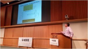
UC Berkeley Professor Alex Zettl described the unique devices his lab has constructed. Shown here presenting to the group at IBM, Prof. Zettl shows his radio receiver based on a single nanowire performing as an antenna with field emitter integrated tuner and amplifier. His Graphene sheet speaker and microphone are distortion free well into the ultrasonic.
IBM Research Almaden’s Director of Science and Technology Dr. Spike Narayan described how nanotechnology and nanoscience are at the core of materials innovations that will be needed to address the current global challenges of clean water, green energy, sustainable environment and effective health care. His work is driven by the belief that the key to disruptive innovation is collaboration among companies as well as multidisciplinary education coupled with computational analysis used to accelerate discovery at a fraction of the current cost.
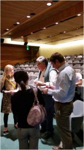
Here an IBM world expert in computational analysis took time to network and answer questions by student attendees.
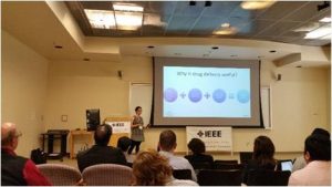
Dr. Kayte Fischer, a recent UC Berkeley grad and Co-Founder and CTO of her own medical devices company Nano Precision Medical, describes her first product, an implantable drug delivery capsule the size of a grain of rice that uses a titania nanoporous membrane to control the rate of drug delivery. The attendees could relate to a female engineering role model and appreciated her tales of her struggles to get her startup off the ground and focused on the right product.
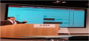
Here NTC Distinguished Lecturer and University of Southern California Professor Wei Wu showed how nanoimprint lithography can be used to fabricate line/space patterns of a few nanometers when its associated mask/mold is made with a beam of single Helium atoms.
Dr. Luisa Bozano, a Research Scientist at IBM Almaden, who is discovering and developing methods for making self-assembled molecular devices, described the importance of becoming an intern and gave advice based on her own experiences working with interns. An attendee named Emily, a grad student at UC Santa Cruz wrote to Dr. Bozano: “I just wanted to send you a note of appreciation for taking time out of your schedule to present at the IEEE conference two days ago. I’ve heard a good amount of advice that parallels yours, but you did an excellent job putting an inspiring personal touch on it, telling stories of your personal experience with many interns, the people who have interacted with you (in good and bad ways), and your own personal successes and failures while early in your career. I’m still at a very early stage in my career, only having done academic research since grad school, but the suggestions you gave were still no doubt useful. I’m currently trying as hard as I can to tunnel through that potential barrier separating me from that industry career that I’m interested in, and I am glad I came up from Santa Cruz to take in advice from you, from the other speakers, and even from the audience members you called on to tell their experiences.”
Holding the last day at Stanford University facilitated the participation of Dr. Arun Majumdar, who has settled into the ME Department after being the Founding Director of the Advanced Research Projects Agency – Energy (ARPA-E) during the first Obama term where he also served as Acting Under Secretary of Energy. He sees nanotechnology playing a big role in how we mitigate the impact of carbon in the atmosphere and how we adapt to it. He also sees it as a game changer that will help enable access to affordable energy in less affluent regions.
All told there were sixteen speakers, eight of whom were from industry and the remainder being academics with current nanotechnology research programs. Their presentations can be found at the IEEE San Francisco Bay Area Nanotechnology Council Chapter’s website www.ieee.org/nano. I could say the event overachieved but that is better left to the attendees to tell. “I have learned a lot from these events and I appreciate all of the work that goes into organizing them”. Erica, UC Berkeley. “It’s definitely convinced me to become an IEEE member.” Gauri, Undergrad, Foothill College


