
Highlights of IEEE Nanotechnology Magazine (December 2015 ISSUE)
Highlights of IEEE Nanotechnology Magazine (December 2015 Issue)
Subscription of the Magazine is welcome!
- Magneto-tunneling junction logic and memory
Supriyo Bandyopadhyay1 and Jayasimha Atulasimha2
1Department of Electrical and Computer Engineering, Virginia Commonwealth University, Richmond, VA 23284, USA
2Department of Mechanical and Nuclear Engineering, Virginia Commonwealth University, Richmond, VA 23284, USA
The rapid increase in demand for computational and signal processing prowess calls for radical and revolutionary advances in reliable, energy-efficient and dense computing architectures. The traditional complementary metal oxide semiconductor field effect transistor (CMOS) based processors are hardly up to the task because of the excessive energy dissipation that they are burdened with and the fact that CMOS is volatile and thereby inherently incapable of storing data indefinitely. All charge based devices like CMOS are hamstrung by unavoidable (and yet unnecessary) energy dissipation. In digital applications, the digital binary bits 0 and 1 are encoded in two different charge states of the device: more charge in the device represents bit 0 (the transistor in ‘ON’) and less charge in the device represents bit 1 (the transistor is ‘OFF’). Since charge is a scalar quantity with magnitude but no direction, encoding two different bits in charge can only happen if they are encoded in two different magnitudes (or amounts) of charge and . Every time the device is switched to toggle the stored bit, the amount of charge in the device must be changed, resulting in an average current to flow through the device if the time taken to switch is. This results in unavoidable energy dissipation where R is the resistance in the path of the current and . If the transistor is switched faster, the energy dissipation increases. If the transistor is operated in a noisy environment, then maintaining distinction between the bits mandates a larger difference between the amounts of charge , which also increases the dissipation.
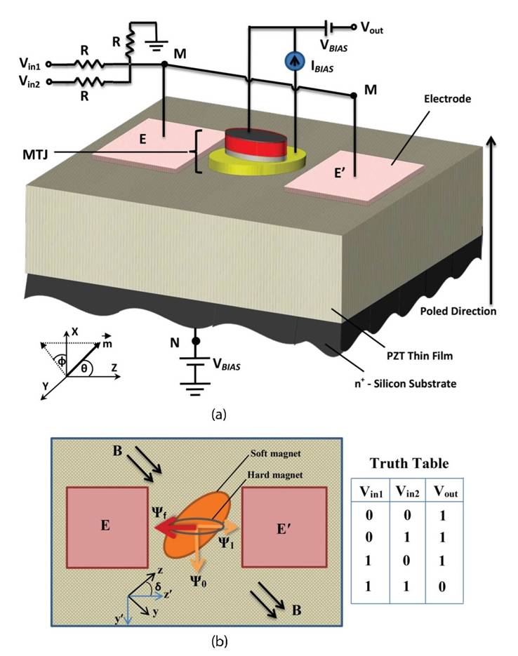
An MTJ-based NAND gate.
The top figure shows the plan view and the bottom figure the top view. The MTJ stack is “skewed”, meaning that the hard and soft layer major axes are not collinear. The soft layer is larger and has more eccentricity than the hard layer. A permanent magnetic field is directed along the minor axis of the soft layer which makes its two stable magnetization orientations point along two mutually perpendicular directions and. The input and output bits are encoded in voltage levels. The two inputs are Vin1 and Vin2 whereas the output voltage is Vout. Reproduced with permission from ref. [35].
- Effects of Film viscosity Changes on the
Electric field-induced Alignment of Graphene flakes in B-stage Graphene-epoxy Composite Films
Seung-Yoon Jung and Kyung-Wook Paik*
Nano Packaging and Interconnect Lab. (NPIL)
Department of Materials Science and Engineering
Korea Advanced Institute of Science and Technology (KAIST)
291 Daehak-ro, Yuseong-gu, Daejeon, 305-701, Korea
*phone: +82-42-350-3335, fax:+82-42-350-8124
e-mail: kwpaik@kaist.ac.kr
Graphene, which is a layer of carbon atoms in a hexagonal lattice, has been reported to have excellent mechanical, electrical, thermal, and gas barrier properties. One of the most widely used applications of graphene is graphene-polymer composites, which are one of the most promising materials because highly functional materials can be produced with small amount graphene flakes incorporated in lightweight polymer matrix. Graphene-polymer composites have been investigated for various kinds of applications such as thermal interface materials (TIMs), electromagnetic interference (EMI) shielding materials, gas sensor materials, and gas barrier materials. [1-2]
In this article, effects of time-temperature dependent viscosity changes on electric field-induced alignment of graphene flakes in B-stage graphene-epoxy composite film were investigated. The alignment direction was parallel to the composite film (horizontal direction). Electric fields were applied to the graphene-epoxy composite film at various temperatures and times. The aligned graphene structure was characterized in terms of film morphology and electrical resistance.
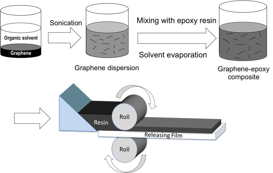
Schematic illustration of B-stage graphene-epoxy composite film fabrication processes.
- Improved Hydrolytic Stability and Repeatability of pH Sensing with APTES-Coated Si Nanowire Bio-FETs
Pengyuan Zang, Student Member, IEEE, Yuchen Liang, Student Member, IEEE, and Walter Hu, Senior Member, IEEE
All authors are with the Electrical Engineering Department, the University of Texas at Dallas, Richardson, TX 75080 USA (email: pxz110730@utdallas.edu; yxl105020@utdallas.edu; walter.hu@utdallas.edu).
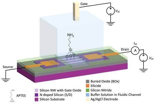
Schematic of the pH sensing setup for the APTES-coated Si NGFET.
This work addresses the hydrolytic instability issue of surface chemistry and repeatability issue of Si nanowire biosensors. Si multi-nanowires or nanograting FETs were fabricated using semiconductor lithographic processing techniques. Then, the nanograting surfaces were coated with 3-aminopropyltriethoxysilane (APTES) via vapor phase and solution phase methods. Their performance including drift, stability, sensitivity, accuracy and linearity of pH sensing was evaluated. Sensors treated with both APTES deposition methods exhibit linear pH response with good sensitivity. Devices treated with vapor APTES shows better linearity and sensitivity, yet solution APTES coated devices are more stable with smaller drift. A hydrolysis process was developed to significantly improve the hydrolytic stability of the APTES coated sensor surface. As a result, an accuracy of ± 0.008 pH was achieved which is comparable or better than commercially available ISFETs, whereas the sensor drift was significantly reduced for both sensors treated with vapor and solution APTES. This hydrolysis process has greatly improved the stability and repeatability of charge sensing of our Si nanograting bio-FETs.