Announcing IEEE-NTC Fall School 2018 on “Nanotechnology for Energy”
When: October 13 and 14, 2018 (prior to IEEE-NMDC 2018)
Location: Engineering Lecture Theater at Portland State University,
Room EB-102, Engineering Building, 1930 SW 4th Avenue, Portland, OR
Fees: $25 (Pre-registration thru 4-Oct) + $35 (after 4-Oct & On-Site)
Registration includes Breakfast and Lunch and lecture materials.
REGISTRATION OPEN https://www.regonline.com/nanoforenergyfall2018
Download PDF flyer
About the School:
This school provides an overview of next-generation nanotechnology solutions / tools for diverse energy applications, and is structured for a target audience of students at the senior-undergraduate and graduate levels. The content will be delivered through 7 synergistic tutorials that focus on the following thematic topics: (i) nanomaterials for energy and sustainability, (ii) nanotechnology for photovoltaics and storage (batteries), and (iii) atomic-to-nanoscale computational modeling / experimental characterization tools for energy nanosystems.
See details on speakers and bios.
Co-sponsored by the IEEE Nanotechnology Council (IEEE-NTC) and the
Department of Electrical & Computer Engineering, Portland State University
Agenda
Technical Program – Day 1
10/13/2018 (Saturday)
| Time | Tutorial Topic / Activity |
| 7:30 – 8:30 | Registration & Breakfast |
| 8:30 – 10:20 | Introduction to Nanotechnology and Nanomaterials
University of Illinois at Chicago, USA |
| 10:30 – 12:20 | Sustainable Materials for Energy Conversion and Storage
Polytechnique Montreal, Canada |
| 12:30 – 13:30 | Lunch |
| 13:30 – 15:20 | Nanotechnology for Photovoltaics
Arizona State University, USA |
| 15:30 – 17:20 | Nanodielectrics and Nanocomposites
École de technologie supérieure (ETS), Montréal, Canada |
Technical Program – Day 2
10/14/2018 (Sunday)
| Time | Tutorial Topic / Activity |
| 7:30 – 8:30 | Breakfast |
| 8:30 – 10:20 | Nanotechnology for Energy Storage
National Cheng Kung University, Taiwan |
| 10:30 – 12:20 | Imaging and Characterization of Energy Nanosystems
University of Illinois at Chicago, USA |
| 12:30 – 13:30 | Lunch |
| 13:30 – 15:20 | Computational Modeling of Energy Nanomaterials
Dr. Arun Kumar Mannodi-Kannakkithodi Argonne National Laboratory, USA |
Speakers:
Introduction to Nanotechnology and Nanomaterials
Prof. Arun Subramanian,University of Illinois at Chicago, USA
Abstract:
This tutorial is designed to provide an introductory overview of the broad field of nanotechnology and nanomaterials. Topics covered will include the following: (i) benefits and rationale for miniaturization, (ii) size effects and impact of scaling laws on the properties and phenomena that obtain at the nanoscopic size regime, (iii) potential nanomaterial systems and their synthesis processes, (iv) characterization techniques and tools for nanoscopic materials, devices, and phenomena, and (v) current / next-generation applications of nanotechnology. The material will benefit aspiring nanotechnologists and offer an introductory background for the advanced topics that follow within the Fall School program.
 Arunkumar Subramanian is currently an Associate Professor in Mechanical and Industrial Engineering at the University of Illinois at Chicago (UIC). His group performs research on nanotechnology solutions for energy and nanomanufacturing applications. He received his doctoral degree from the Institute for Robotics at the ETH in Zurich and has held a post-doctoral appointment at the Sandia Labs in Albuquerque. He studied mechanical engineering at the University of Minnesota and at the Birla Institute of Technology and Science (India), and has previously worked at the Honeywell R&D Labs. His work has been published in journals such as ACS Nano, Science, Nanoscale, Nano Today and Applied Physics Letters, among others, and has resulted in three US patents. He is a recipient of the NSF CAREER award, and currently serves as the Vice President for Education within the IEEE Nanotechnology Council.
Sustainable Materials for Energy Conversion and Storage
Prof. Clara Santato, Polytechnique Montreal, Quebec, Canada
Abstract:
Electronics have become indispensable in our daily routine. A great part of the electronic equipment that surrounds us belongs to what is known as conventional electronics, based on inorganic materials such as silicon and gallium arsenide.
However, with the life of the electric and electronic equipment becoming shorter and shorter, two major issues arise for both the scientific community and municipalities: the increasing amount of Waste of Electrical and Electronic Equipment (WEEE) and the depletion of natural resources. Taking into account the definition of sustainability provided by the United Nations (the ability of satisfying one generation’s needs without compromising the possibility of future generations to satisfy), those two issues point to the lack of sustainability in the electronics field of the current generation, at least so far. Consequently, great attention has been given to green (sustainable) electronics in the last years, having as core values (i) the use of abundant and low-cost precursors, leveraging on processing routes that (ii) lack toxic solvents as well as toxic waste and (iii) are low cost and (iv) involve biodegradable materials.
We will include in the presentation our preliminary results on the biodegradability and compostability of organic electronic materials of interest for electronics and energy storage devices, focusing on the case of study of melanin biopigments used in transistors, batteries and supercapacitors [1].
[1] E. Di Mauro, R. Xu, G. Soliveri, C. Santato, Natural melanin pigments and their interfaces with metal ions and oxides: emerging concepts and technologies, MRS Commun. 7 (2017) 141–151. doi:10.1557/mrc.2017.33.
Clara Santato earned her PhD degree in chemistry in 2001 from the Université de Genève and her MSc degree in chemistry in 1995 from Università degli Studi di Bologna. She was a (permanent) research scientist at the Institute for Nanostructured Materials, part of the Italian National Research Council, from 2001 to 2011, and a visiting scientist at Purdue University, Cornell University, Institut National de la Recherche Scientifique, McGill University and Cornell University.
Santato’s research focuses on semiconducting films and their interfaces with electrodes and electrolytes, for applications in transistors and energy conversion/storage, and has been recently recognized by her elevation to the Institute of Electrical and Electronics Engineers (IEEE) senior membership.Santato is a member of the UNESCO MATECSS (Materials and Technologies for Energy Conversion, Saving and Storage) Chair. She serves as editor of the Journal of Power Sources (Elsevier).
Nanotechnology and Next-Generation Photovoltaics
Prof. Stephen Goodnick, Deputy Director, QESST Engineering Research Center, School of Electrical Computer and Energy Engineering, Arizona State University, USA
Abstract:
This tutorial will set the stage for understanding and appreciating the latest advances and central challenges in photovoltaics research. Over the long term, nanotechnology is expected to enable improvements throughout the energy sector, but the most striking near- to mid-term opportunities may be in lower-cost, higher-efficiency conversion of sunlight to electric power. Nanostructures in solar cells have multiple approaches by which they can improve photovoltaic performance: (1) New physical approaches in order to reach thermodynamic limits; (2) Allow solar cells to more closely approximate their material-dependent thermodynamic limits; and (3) Provide new routes for low-cost fabrication by self-assembly or design of new materials. We focus primarily on the first two approaches which have the goal of increasing efficiency. We first discuss how quantum wells, nanowires and quantum dots are incorporated into conventional solar cell structures, and the performance of such approaches to date. In this context, we focus on the effects that surfaces and interfaces play in nanostructured solar cells, and how to reduce parasitic carrier recombination effects through passivation. We also discuss the role of nanotechnology in improving light trapping and the light collection properties of solar cells. Finally, several different approaches will be described that circumvent long-held physical assumptions and lead beyond first- and second-generation solar cell technologies. Special emphasis will be on novel nanostructure-based devices based on advanced concepts such as hot carrier cells, intermediate band and multi-exciton generation, which have the theoretical basis to realize high efficiency energy conversion.
 Stephen M. Goodnick received his Ph.D. degrees in electrical engineering from Colorado State University, Fort Collins, in 1983, respectively. He was an Alexander von Humboldt Fellow with the Technical University of Munich, Munich, Germany, and the University of Modena, Modena, Italy, in 1985 and 1986, respectively. He served as Chair and Professor of Electrical Engineering with Arizona State University, Tempe, from 1996 to 2005. He served as Associate Vice President for Research for Arizona State University from 2006-2008, and presently serves as Deputy Director of ASU Lightworks. He was a Hans Fischer Senior Fellow with the Institute for Advanced Studies at the Technical University of Munich, 2013-2017. Professionally, he served as President (2012-2013) of the IEEE Nanotechnology Council, and served as President of IEEE Eta Kappa Nu Electrical and Computer Engineering Honor Society Board of Governors, 2011-2012. Some of his main research contributions include analysis of surface roughness at the Si/SiO2 interface, Monte Carlo simulation of ultrafast carrier relaxation in quantum confined systems, global modeling of high frequency and energy conversion devices, full-band simulation of semiconductor devices, transport in nanostructures, and fabrication and characterization of nanoscale semiconductor devices. He has published over 400 journal articles, books, book chapters, and conference proceeding, and is a Fellow of IEEE (2004) for contributions to carrier transport fundamentals and semiconductor devices.
Nanodielectrics and Nanocomposites
Dr. Michel Fréchette, École de technologie supérieure (ETS), Montréal, Canada
Abstract:
After a noticed introduction of the “nanodielectric” concept in 2001, a continuous increase of scientific progress and development in this field has been observed. Important sessions of international scientific conferences are now devoted to nanodielectrics and/or nanomaterials for electrotechnical applications.
These years of research have allowed to demonstrate the possibilities of tailoring the macroscopic material properties at the nanoscale and shown that the dielectric properties could be affected and improved. Nowadays, it can be said that a second-generation wave of nanodielectrics is being developed and studied. Relative to these advanced materials, fabrication and processing take more place in determining the properties exhibited by the prepared materials.
Time permitting, polymer dielectrics will be discussed followed by the introduction of nanodielectrics. After these items, a snapshot of the current achievements involving polymer nanocomposites will be given. Possibilities of tailoring the dielectric functions of polymer nanocomposites will be made explicit and exemplified. Finally, the case involving Graphene forming composites with polymers will be explored and an overview of current applications of nanodielectrics for high-voltage applications will be presented.
Force is to conclude that the insofar situation is still very much empirical.
 Michel Fréchette is a physicist who spent most of his carreer at Hydro-Québec’s research institute (IREQ), Varennes, Qc, Canada. As an industrial scientist, Dr. Fréchette has been involved in applied basic research in various fields related to electrical insulation, insulating materials and nanodielectrics. He was subsequently a full-time Visiting Professor at the Xi’an Jiaotong University (XJTU), Xi’an, China. He is now Associate Professor at École de technologie supérieure (ETS) in Montréal, Qc.
Nanotechnology for Energy Storage
Prof. Yonhua Tzeng, National Cheng Kung University, Taiwan
Abstract:
Nanoscale materials and structures have been extensively studied for enhancing the performance of existing energy storage technologies or enabling new and better means of storing energy. Among energy storage devices, rechargeable batteries, super capacitors, and their combinations for practical applications will be discussed. In the first half of this lecture, basic operational principles of various kinds of batteries and super capacitors will be explained with an aim at familiarizing students and professionals who are not currently actively working in this field with fundamental knowledge in preparation for conducting related research. More details will then be discussed about how nanotechnology and nanoscale materials and structures are being applied to improve or enable energy storage of higher capacity, longer lifetime, and safer uses for better humanity.
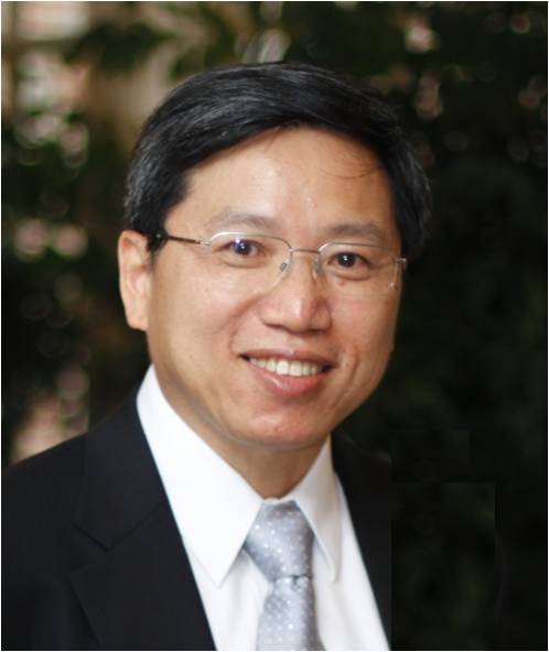 Yonhua Tzeng is currently University Chair and Distinguished Professor of Electrical Engineering at National Cheng Kung University in Tainan City, Taiwan, where he served as former Dean of College of Electrical Engineering and Computer Science and former Vice President for Research and Development. Professor Tzeng currently serves as President of IEEE Nanotechnology Council. Professor Tzeng is a professor emeritus of Department of Electrical and Computer Engineering, Auburn University, Auburn, Alabama USA. His research interests include materials of extreme properties and practical applications, especially carbon materials for energy storage, photonics, sensors and electronics. Professor Tzeng has published more than 200 journal and conference papers and been awarded more than 40 patents.
In-Situ Transmission Electron Microscopy Studies of Energy Storage Materials
Prof. Reza Shahbazian-Yassar, University of Illinois at Chicago, USA
Abstract:
An in-depth understanding of material behaviors under complex electrochemical environment is critical for the development of advanced materials for the next generation rechargeable ion batteries. Real-time transmission electron microscopy (TEM) of electrochemical reactions is one of the most significant breakthroughs poised to enable radical shift in our knowledge on how new materials behave in electrochemical environment. This presentation gives an overview of the PI’s efforts on understanding the atomistic mechanisms behind the charge storage and thermal runaway in rechargeable ion batteries. Topics related to the interaction of ionic transport and microstructural features (e.g. twin boundaries), atomic tunnels, and crystallographic misorientations will be covered. In addition, we reveal new mechanisms by which alloying reactions and conversion reactions proceed in new anode materials such as phosphorene and Sb-based alloys. At the end, we will discuss new opportunities enabled by in-situ TEM to advance the current state of battery materials.
Dr. Reza Shahbazian-Yassar‘s research focus is on understanding the behavior of functional nanomaterials under dynamic environment such as exposure to gas, electrical/thermal field, electrochemistry, and liquid solutions. He has published more than 150 peer-reviewed journal articles in leading journals such as Science, Nature Energy, Nature Communications, etc. He served as the President of the Midwest Microscopy Society and also the Materials Science Director at the Midwest Microscopy Society. He also served as the Chair and Vice Chair of Advanced Characterization, Testing, and Simulation Committee at the Materials, Metals, Minerals Society (TMS). He has hold various officer positions at the Microscopy Society of America and the Nanoengineering for Energy and Sustainability Committee at ASME society.
Computational Modeling of Energy Nanomaterials
Dr. Arun Kumar Mannodi-Kannakkithodi, Argonne National Laboratory, USA
Abstract:
The notion of designing materials on a computer before a single laboratory experiment is conceived was a game changer in the field of materials science and engineering. The advent of supercomputers along with theoretical advancements in classical and quantum mechanics, formulations of force-field simulations and molecular dynamics, and the development of quantum mechanics-based methods like density functional theory (DFT) formally kick-started the era of computational materials science. Quantum mechanics, in particular, provided a fundamental look at the structure and properties of materials in the smallest available length and time scales, and made for accurate (but computationally expensive) solutions of many material science problems. Today, DFT is being widely used to study the mechanical, electronic, dielectric and thermodynamic properties of metals, inorganic compounds, molecules and polymers. DFT can be credited with driving rational materials design by eliminating guesswork from experiments; some prominent examples include the identification of new cathode materials for Li batteries, the design of novel NiTi shape-memory alloys, the discovery of previously unknown ABX type thermoelectrics and conductors, and the design of novel polymeric capacitor dielectrics. Further, the increasing application of computational methods in a high-throughput and automated fashion has led to the creation of massive materials datasets, which can be mined to yield correlative relationships, chemical design rules and predictive models. Indeed, machine learning (ML) techniques have been applied to computational (as well as experimental) data to yield more accurate energy and force predictions, to predict properties of materials in an on-demand fashion, and for design of experiments.
In this lecture, I will go through the different scales of materials modeling (continuum, classical, quantum), with a special emphasis on DFT: the basic formalism, the levels of theory, and application to crystalline materials. I will further describe the application of machine learning to materials science data, highlighting several important regression and classification algorithms used and the fingerprinting of materials, that is, converting any dataset of materials into unique numerical representations based that can be mapped to the properties of interest to yield learning models. I will delve into two major examples to explain the successful application of DFT and ML for accelerated materials design: the rational design of polymer dielectrics, and the prediction of point defect levels in semiconductors. I hope to demonstrate through these examples how to conceive the solution of a materials science problem using computational techniques, how to work closely with experimentalists to guide the synthesis and design of new candidate materials, and how to expand knowledge to hitherto unexplored areas of the chemical space by learning from computational data. It should be noted that there has been a recognition of the power of computations and databases in guiding the rational experimental design of materials in the form of the Materials Genome Initiative10, which was announced by the US government ‘‘to discover, manufacture and deploy advanced materials twice as fast, at a fraction of the cost’’. High performance computing, efficient computational approaches and machine learning based methods provide great promise in accelerating the pace of discovery and deployment of new materials in practice.
Dr. Arun Kumar is a postdoctoral researcher in the Theory and Modeling Group at the Center for Nanoscale Materials in Argonne National Laboratory. He received his Bachelor of Technology in Metallurgical and Materials Engineering from the Indian Institute of Technology, Roorkee, India in 2012, and joined the Materials Science and Engineering department in University of Connecticut, CT, USA for a PhD the same year. His doctorate was completed in 2017 under the supervision of Prof. Rampi Ramprasad with a dissertation titled “Rational design of polymer dielectrics using density functional theory and machine learning”. His expertise is in applying first principles computations and machine learning techniques to study the electronic, dielectric and defect properties of crystalline materials, and in guiding rational experiments for the discovery of new materials. At Argonne, his research is focused on computation and machine learning driven predictions of defect properties in various classes of semiconductors like hybrid organic-inorganic perovskites and chalcogenides.