 IEEE Nanotechnology Magazine, all about nanotechnology,sponsored by IEEE Nanotechnology Council for the world-wide nanotechnology community is featuring the following highlighted articles on nanotechnology:
1. West, A.; Griep, M. ; Cole, D. ; Karna, S. Gold Nanocluster DNase 1 Hybrid Materials: An Efficient Method for DNA Contamination Sensing. IEEE Nanotechnology Magazine, Vol. 9, Issue 1, pp. 25-30, March 2015. http://dx.doi.org/10.1109/MNANO.2014.2373452
Protein-encapsulated g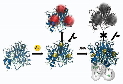 old nanocluster (P-AuNC) synthesis was first demonstrated in 2009 [1]. Initially, these P-AuNCs were used as cellular imaging agents as the protein shell surrounding the AuNC made them highly biocompatible. However, recent studies have begun to show that these stabilizing proteins may also retain native biological function, thus giving a dual functionality to these hybrid molecules. Here, we present the synthesis of DNase 1 stabilized AuNCs (DNase 1:AuNCs) with core sizes consisting of either eight or 25 atoms. The DNase 1:Au8NCs exhibit blue fluorescence, whereas the DNase 1:Au25NCs are red emitting. Moreover, in addition to the intense fluorescence emission, the synthesized DNase 1:AuNC hybrids retain the native functionality of the protein, allowing simultaneous detection and digestion of DNA with a detection limit of 2 mg/mL (Figure 1). The DNase 1:AuNCs could be conveniently employed as efficient and fast sensors to augment the current inefficient and time-consuming DNA contamination analysis techniques.
2. Streller, F. ; Wabiszewski, G. ; Carpick, R. Next-Generation Nanoelectromechanical Switch Contact Materials: A Low-Power Mechanical Alternative to Fully Electronic Field-Effect Transistors. IEEE Nanotechnology Magazine, Vol. 9, Issue 1, pp. 18-24, March 2015. http://dx.doi.org/10.1109/MNANO.2014.2373451
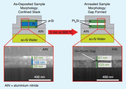 The deficiency of existing electrical contact materials is currently a significant impediment to the commercialization of nanoelectromechanical (NEM) contact switches, a low-power beyond complementary metal-oxide semiconductor (CMOS) technology? NEM switches using traditional metallic electrical contact materials, even those composed of inert, noble metals such as gold (Au) and platinum (Pt), demonstrate premature failure due to either their adhesiveness or catalytic activity, leading to a buildup of insulating interfacial contaminants. Commercially viable NEM switches demand novel contact materials along with efficient methods to evaluate the performance of these materials.
3. Tao, J. ; Mathewson, A. ; Razeeb, K. Nanowire-Based Anisotropic Conductive Film: A Low Temperature, Ultra-fine Pitch Interconnect Solution. IEEE Nanotechnology Magazine, Vol. 9, Issue 1, pp. 4-11, March 2015. http://dx.doi.org/10.1109/MNANO.2014.2373531
Advanced microelectronic s packaging, driven by the multiple benefits of system performance, power, size, and cost, has now entered the three-dimensional (3-D) era. According to the International Technology Roadmap for Semiconductors 2012, the interconnect pitch size is predicted to be 4-16um at the global interconnect level by the year 2018. Silicon die incorporated with through-silicon-via (TSV) technology can be stacked using solder microbumps as high-density interconnects. However, solder microbump technology faces many challenges because of the intermetallic compound growth and an underfill requirement as the bump size reduces. Meanwhile, the temperature of the soldering process is more than 260C, which can result in high thermal stress in the devices and impact the thermal budget of the processing, particularly for the multitechnology node-stacking processes. Therefore, developing interconnect methods, which can provide ultrafine-pitch capability and low-temperature process for 3-D systems, attracts continuous attention from industry.
4. Ji, Y. ; Hu, J. ; Lanza, M. A. Future Way of Storing Information: Resistive Random Access Memory. IEEE Nanotechnology Magazine, Vol. 9, Issue 1, pp. 12-17, March 2015. http://dx.doi.org/10.1109/MNANO.2014.2373402
Electronic informa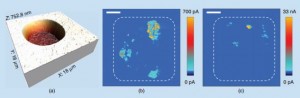 tion storage has become one of the major needs of modern societies, and it represents a market of more than US$5 billion. Among all of the existing technologies, flash memory is the most widespread because of its simple structure, high integration, and fast speed. The core cell of this device is based on the charge and discharge of a capacitor using a transistor as a tiny switch, but, as the devices are scaled down, this configuration presents some physical limitations. Therefore, new ways for information storage are required, and, among all existing nonvolatile memories, one that has raised major expectations in recent years is resistive random access memory (RRAM). In this article, we present the working principle and functioning of the most promising RRAM devices for future information storage.
[…] access journal) and T-MBMC went live with their manuscript submission sites; the March issues of IEEE Nanotechnology Magazine and TNANO were published; TNB transitions to 8 online issues per year; a NTC Summer School on […]