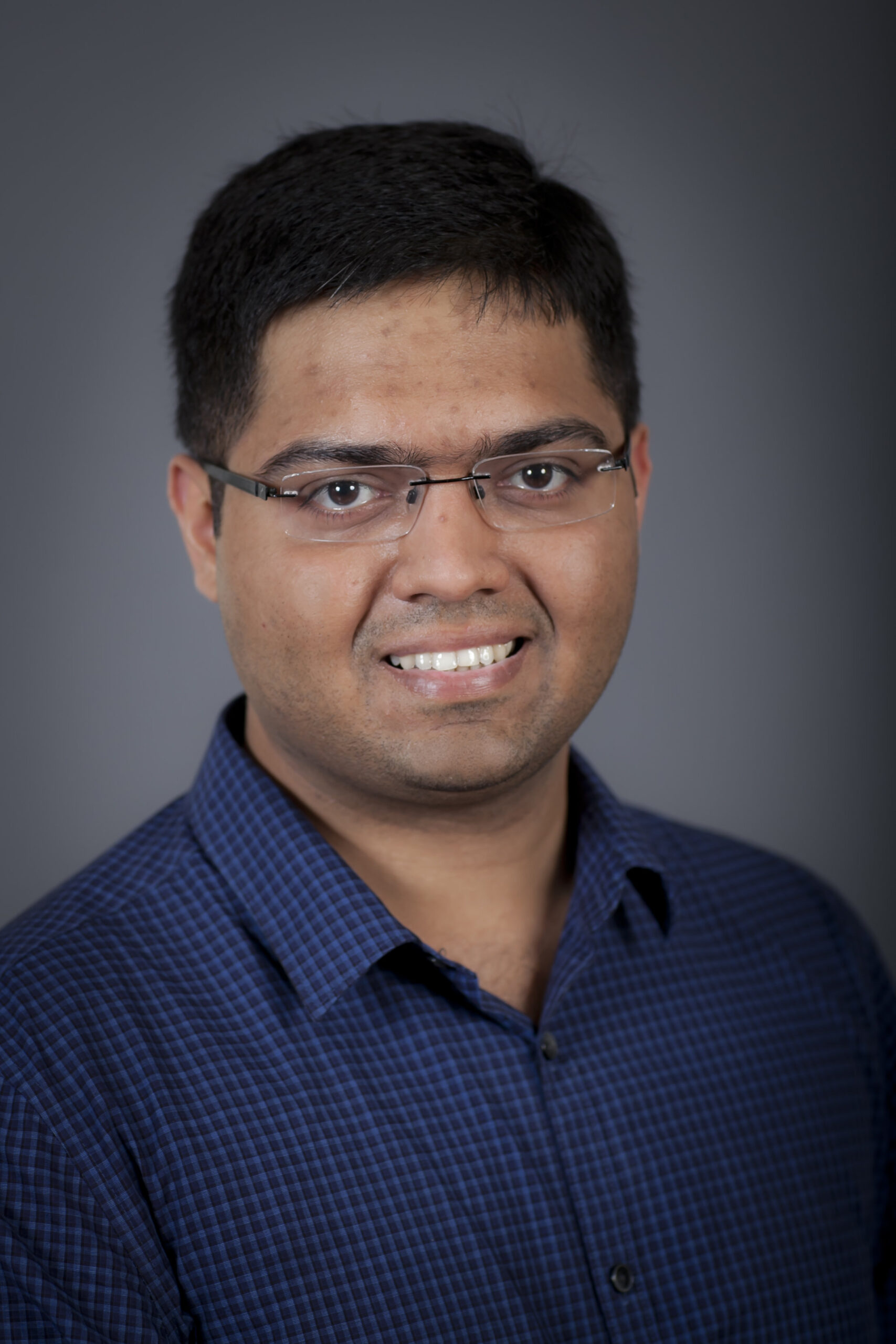
Deep Jariwala is an Assistant Professor in Department of Electrical and Systems Engineering at the University of Pennsylvania (Penn). His research interests broadly lie at the intersection of new materials, surface science and solid-state devices for computing, sensing, opto-electronics and energy harvesting applications. Deep completed his undergraduate degree in Metallurgical Engineering from the Indian Institute of Technology, Banaras Hindu University in 2010. Deep went on to pursue his Ph.D. in Materials Science and Engineering at Northwestern University working on charge transport and electronic applications of two-dimensional (2D) semiconductors, graduating in 2015. Deep then moved to Caltech as a Resnick Prize Postdoctoral Fellow from 2015-2017 working on nanophotonic devices and ultrathin solar cells, before joining Penn in 2018 to launch his independent career.
Deep’s research has earned him awards of multiple professional societies including the Russell and Sigurd Varian Award and Paul H. Holloway Award of the American Vacuum Society, The Richard L. Greene Dissertation Award of the American Physical Society, Johannes and Julia Weertman Doctoral Fellowship, the Hilliard Award, the Army Research Office and Office of Naval Research Young Investigator Awards, Nanomaterials Young Investigator Award, TMS Frontiers in Materials Award, Intel Rising Star Award, IEEE Young Electrical Engineer of the Year Award, IEEE Photonics Society Young Investigator Award, IUPAP Early Career Scientist Prize in Semiconductors, IEEE Nanotechnology Council Young Investigator Award in addition to being named in Forbes Magazine list of 30 scientists under 30, is an invitee to Frontiers of Engineering conference of the National Academy of Engineering as well as a recipient of the Sloan Fellowship. Recently, his work on ferroelectric diode memory was also awarded with the Bell Labs Prize. In addition, he has also received the S. Reid Warren Jr. award given to one faculty member every year at Penn Engineering for inspiring and motivating undergraduate students through teaching. He also serves as Associate Editor for IEEE Photonics Technology Letters as well as npj 2D materials and applications. He has published over 100 journal papers with more than 16000 citations and several patents. At Penn he leads a research group comprising more than ten graduate and postdoctoral researchers supported by a variety of government agencies, industries and private foundations.
Google Scholar | Lab website | LinkedIn
Tell us a little bit about your educational/professional background. How are you involved in IEEE NTC Modeling and Simulation?
I grew up in Mumbai, India and went to high school there. I then went to the Indian Institute of Technology at Banaras Hindu University (IIT-BHU) in Varanasi for my bachelor’s degree in Metallurgical Engineering. During my undergraduate degree, I spent two summers at Rice University which sparked my interest in nanotechnology and nanomaterials. After finishing my undergraduate, I went straight to PhD in Materials Science and Engineering at Northwestern University where I worked on novel types of transistors and diodes using two-dimensional (2D) and one-dimensional (1D) semiconductors. During PhD was the first time I got exposed to device modelling and simulation. After PhD, I kept working on devices but moved to Caltech to pursue a postdoctoral position in photonic and optoelectronic devices. At Caltech, I was exposed to the electromagnetic wave and optical simulations. Starting 2018, I moved to the University of Pennsylvania to start my independent research group where we work on both electronic and photonic devices from novel nanomaterials. We make and measure devices as well as simulate and predict their performance.
What is your primary research interest? What are the major areas that your research group works on?
My research interests are extremely broad. But the primary objectives can be summarized as using new materials for novel devices involving computing, communication, sensing and energy harvesting applications. Presently, there are 4 major areas of the research group:
- Nanoelectronics: In this area, we work on novel logic transistors as well as novel non-volatile memory devices. We also focus on fundamental device challenges such as contact resistance as well as think about circuits and system-level implementation of new devices.
- Nanophotonics/Optoelectronics: In this area, we focus on low-dimensional materials with novel optical properties and structure them to trap light and observe novel photonic phenomena. We are also equally interested in using the observed novel photonic phenomena in device applications.
- Functional imaging: In this area, we focus on electron beam and scanning probe-based imaging of new materials, heterostructures and their interfaces. We call this area functional imaging since we are doing more than just standard imaging by applying another stimulus during imaging. For example: applying heat or electric field or magnetic field during e-beam imaging or shining light or applying voltage during scanning probe imaging.
- Synthesis of new semiconductor materials: In this area, we use vapour phase and plasma phase deposition techniques to grow new semiconductors and their heterostructures and investigate their fundamental crystal, electronic and optical properties.
Lead us through your Academic Career Highlights and share your experience.
I was always inclined towards high education and deep scientific inquiry. I’d say all the way from my middle school days if my memory serves me correctly. The first major highlight was going to IIT for undergraduate education. There I came in contact with some professors and other senior students who encouraged me to go into research and pointed me in the right direction.
At IIT-BHU, I started doing some molecular dynamics simulations research which led to a summer internship at Rice University. That was another major highlight. The Rice experience opened doors to experimental, physical lab-based research which was very instrumental and eye-opening in terms of my thinking and intellectual evolution. After spending two summers at Rice, I decided to apply for PhD program and was fortunate enough to get into Northwestern University in their Materials Science and Engineering PhD program. That was another major highlight.
Northwestern years were very formative in becoming a well-rounded researcher since my PhD advisers at the time gave me all the freedom and resources and provided a very healthy environment to pursue high-risk, high-reward research. That paid off well which led to a productive PhD and a postdoc opportunity at Caltech. Moving to Caltech to work with one of the leading groups in photonics and optical materials was another major highlight. Caltech experience further developed me into an independent scientist and taught me the importance of collaborations as well as marriage between theory and experiments in research.
All these experiences combined led to my current position as a group leader at Penn. Starting an independent lab and career is always challenging and therefore a major highlight. This experience at Penn taught me a lot about how to raise money, manage ideas, people, resources, collaborations and more importantly expectations of everyone. Doing all this successfully and living through a pandemic was quite an experience. An important positive thing I learned managing our lab through the pandemic is to never give up and always keep motivation high among the students and postdocs. I also learned how resilient most of us are as human beings and emerge from all kinds of adversity. Our group emerged quite strong both mentally and scientifically through the pandemic. We had an excellent 2021 and 2022 in terms of publications which led to several awards and honors for the entire group. A major highlight of all these successes was winning the Bell Labs Prize together with my colleagues Troy Olsson and Eric Stach. That one was a very intense competition and the final round involved presenting in front of a judging panel that had multiple CEOs and Nobel laureates. So that whole experience was quite thrilling.
How is your Research Group structured? Is your work done in collaboration with other Industry Partners? If so, what would be your advice to young researchers on strategies to find a good set of collaborations?
Our research group has a very flat structure. Everyone can approach me directly for any advice or help. Of course, some younger students are mentored by senior students or postdocs but everyone gets to talk to me directly. We work as a team and there are really no boundaries between projects. So, if the nanoelectronics folks think there is something cool on the materials or nanophotonics side that they can contribute to, they just go ahead, talk to the relevant group members and collaborate. Sometimes they would run the ideas by me. Other times it is just spontaneous. Similarly, if they want to collaborate with another group at Penn or elsewhere, I proactively make the connections to get the collaboration going. Similar collaborations work with industry and very important government labs as well. In general, we are a very collaborative group and work with dozens of other researchers all over the world. I personally think that is one of our strengths and what makes us so interdisciplinary and productive.
From the viewpoint of someone who has been in academia for many years, how do you think your perspective or approach to research has changed from when you started your PhD work?
To be honest, I haven’t been in academia for very long. Just finishing ~5 years as a group leader/principal investigator. But my research perspective has changed a lot even in this short time. What I have realized over time is that one should always have a big picture of the impact of the research in their minds while working hard and deeply on a problem. The impact may be in community-wide scientific understanding or in terms of tangible technology. Both are fine and equally important. It is also very important to know when to stop working and let things go/end and when to stop, summarize and publish. Scientific world is very big, getting bigger by the day, and more dynamic and fast-moving these days than ever before. So, one needs to be flexible and adapt to these changes which could be both in ways of doing things or in changes to research problems as well.
Do you or your immediate group focus on translating your research into profitable products or is your group mainly involved in exploring more fundamental questions in nanotechnology? If you address fundamental questions, how does your work differ from work done in the industry?
We do both. I would say in the early parts of my career as a student and postdoc I was mostly a fundamental research person. But nowadays we are quite cognizant that many of our ideas could have commercial value and therefore we frequently patent and also think about licensing or starting companies. In terms of fundamental questions, we are looking at basic materials physics/new phenomena questions which are often not being pursued by most industries. Industries, at least semiconductors and optoelectronic industries are focused on optimizing device performance and scaling. They will pick up a problem in most cases when the physics has already been worked out and individual device or materials performance has exceeded certain set benchmarks that are relevant for a technology/product. We do that kind of research as well but then we try and maintain clear boundaries i.e. if there are things that industries are doing can do much better than us since they have more human power and resources, then we would just stay away from such research problems since they go outside the realm of academia at that point, in my personal opinion.
In an academic research centre such as yours, how do you select a research problem to work on? How do you evaluate progress over time?
This is a great question. Selecting research problems is never an easy process. There are always curiosity-driven questions that one has but the issue is how to find funding and resources to execute them. I, therefore, have two classes of problems. The ones that I am more confident about working with and also confident getting funding for them and other class which are riskier and more difficult to get funding on; but very interesting nonetheless. The former ones are straightforward to work on. Define the problem, get some preliminary data, apply for grants and secure funding (this process can be time-consuming and painful sometimes) and then recruit students and execute. The second class of problems are trickier to work on. Typically, I try and search for discretionary funding opportunities or motivated students and postdocs with their own fellowships to work on such problems. Evaluating progress depends on what you want to learn from the problem or what do want as the final result. If the scientific principle you are after is understood, it means progress has been made and you were successful. However, if the end goal is to reach a certain performance or technology demonstration then once again it is very subjective on how you define it. For all highly applied problems, my personal evaluation is that you develop it to a level that someone can make a real technology and product out of it.
Discuss your IEEE journey and motivation to volunteer.
I joined IEEE when I was PhD student. Mainly because I had heard of it since my high school days. Society was somewhat of an enigma for me during college/undergraduate since I thought it was mainly for circuit engineers. Then after I entered PhD program I realized how broad IEEE is and how many societies and technical councils it had and how interconnected/valuable they are in terms of resources and networking. Thereafter, I regularly started following IEEE activities. I think my involvement with the IEEE intensified when I decided to take up a professorship in the Electrical Engineering (EE) department. I had all my degrees in Materials Science and then I took up EE as my home department, which was very rewarding, to be honest. Then, I got involved in IEEE Young Professionals committees, local EDS chapters, EDS optoelectronics committee etc. I also slowly got involved in NTC and in journal editing for the Photonics Society both of which are very rewarding experiences. I would say that there are multiple places in IEEE where I have found a professional home in. EDS, NTC and the Photonics Society are the three most prominent ones. I would say from the disciplinary perspective my research aligns most closely with NTC. Professional societies are meant for professional development and one way to do that is to contribute to them which is to volunteer. Therefore, I encourage everyone to do so in whatever capacity one can manage.
How do you leverage IEEE for your own learning?
My main sources from IEEE for my own learning and professional development are
- Conferences: The content of talks, posters and networking at IEEE conferences is just breathtaking and invaluable.
- Journals: I read a lot of papers and also serve as an associate editor which both contribute a lot to learning about other people’s work and hearing the opinions of others in various research areas of interest.
- Webinars and committees: IEEE webinars are very well advertised and very informative. Similarly, committee meetings give a great chance to learn not just about society but also about other professionals’ career trajectories in your field as well as outside your field.
Which achievement in IEEE/life are you most proud of?
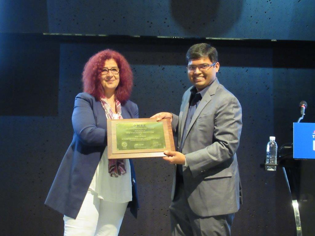
I have a few achievements related to IEEE that I am very proud of. But the latest honor i.e. being named the IEEE NTC Early Career Awardee for 2023 takes the cake. Given the list of former awardees, how much they have achieved in their own careers and how many of them have had an influence on my own scientific thinking and career, this award from the NTC is truly special.

Figure: Dr. Deep Jariwala receiving the IEEE Nano Early Career 2023 award.
Article Contribution: This interview was conducted by IEEE NTC MENED 2022 mentee, Miss Noor E Karishma Shaik and reviewed by Prof. M.P.Anantram from IEEE TC-10 Committee.
 Malgorzata Chrzanowska-Jeske is Professor of ECE and Director of VLSI & Emerging Technology DA Laboratory at Portland State University, where she was ECE Department chair from 2004 to 2010. Previously, she was with the Technical University of Warsaw and the Research and Production Center of Semiconductor Devices. She holds a Ph.D degree in EE from Auburn University. Her research interests include CAD for VLSI and 3DICs, nanotechnology and nano/bio systems, and design for emerging and renewable technologies. She has presented tutorial, keynote, and invited talks at international conferences, published 150+ technical papers, and serves as panelist/reviewer for the National Science Foundation, National Research Council Canada, and international journals and conferences. Her research has been supported by NSF and industry.
 John T. W. Yeow is currently a Professor and a University Research Chair in the Department of Systems Design Engineering at University of Waterloo, Waterloo, ON, Canada. He is focused on the development of micro/nanodevices for a wide range of applications. He is a recipient of the Professional Engineers Ontario Engineering Excellence Award, Natural Science & Engineering Research Canada Innovation Challenge Award, Douglas R. Colton’s Medal of Research Excellence, Micralyne Microsystems Design Award, Ontario Ministry of Research and Innovation’s Early Researcher Award, University of Toronto Alumni Association 7T6 Early Career Award, 2011 IEEE NANO Excellence Paper award and IEEE Canada Outstanding Engineer Award. He was a Canada Research Chair in Micro/Nanodevices (2004 – 2019). He is a Fellow of the Canadian Academy of Engineering, the Engineering Institute of Canada, Engineers Canada, and a Member of College of New Scholars, Artists and Scientists of the Royal Society of Canada.
 Sanjukta Bhanja is a professor in the Electrical Engineering department at the University of South Florida. She earned her bachelor’s degree in EE from Jadavpur University (1991), master’s degree from the Indian Institute of Science (1994), and a PhD in Computer Science and Engineering from the University of South Florida (2002). Currently serving as Engineering’s Executive Associate Dean, Bhanja manages faculty affairs, finance, HR, and space. Her research in nano-electronics and applied physics is supported by the National Science Foundation and NASA. Bhanja has graduated 12 PhD students who work in high-tech industries, and she advises four doctoral students, including three women. Her research has been published in top-tier peer-reviewed journals and conferences like Nature Nanotechnology. Bhanja has received the NSF CAREER award, university-level outstanding research and teaching awards, and the Florida Education Foundation William Jones Outstanding Mentor Award. She is a fellow of the Executive Leadership in the Academic Technology, Engineering, and Science (ELATES at Drexel®) program.
 Li Tao is a full professor at Southeast University, Nanjing, China. His research interests focus on 2D materials and their flexible/wearable devices for health care and internet of things, which had been featured in TIME blog, Nature News and 50+ tech media. He is an inventor of the silicene field-effect transistor and 12’’ wafer-scale graphene on evaporated Cu for GHz flexible RF electronics. He has published 60+ research articles, including first or corresponding author Nature Nanotechnology (citations>1200), Chemical Society Reviews, ACS Nano, Advanced Functional Materials etc., with a h-index 30 and citations ~5000. He is a principle investigator of several research projects with a total funding accumulated over $1.5M. Prof. Tao is an associate editor for Research and Microelectronics Engineering, a committee member for EIPBN (3-beam) conference. He is a senior member of IEEE and NTC Distinguished Lecturer.